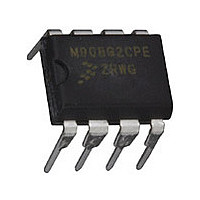
MC68HC908QT2CPE Freescale, MC68HC908QT2CPE Datasheet - Page 101

MC68HC908QT2CPE
Manufacturer Part Number
MC68HC908QT2CPE
Description
Manufacturer
Freescale
Datasheet
1.MC68HC908QT2CPE.pdf
(184 pages)
Specifications of MC68HC908QT2CPE
Cpu Family
HC08
Device Core Size
8b
Frequency (max)
8MHz
Total Internal Ram Size
128Byte
# I/os (max)
6
Number Of Timers - General Purpose
2
Operating Supply Voltage (typ)
3.3/5V
Operating Supply Voltage (max)
5.5V
Operating Supply Voltage (min)
2.7V
On-chip Adc
4-chx8-bit
Instruction Set Architecture
CISC
Operating Temp Range
-40C to 85C
Operating Temperature Classification
Industrial
Mounting
Through Hole
Pin Count
8
Package Type
PDIP
Program Memory Type
Flash
Program Memory Size
1.5KB
Lead Free Status / RoHS Status
Compliant
- Current page: 101 of 184
- Download datasheet (2Mb)
12.3.2 Data Direction Register B
Data direction register B (DDRB) determines whether each port B pin is an input or an output. Writing a 1
to a DDRB bit enables the output buffer for the corresponding port B pin; a 0 disables the output buffer.
DDRB[7:0] — Data Direction Register B Bits
When DDRBx is a 1, reading address $0001 reads the PTBx data latch. When DDRBx is a 0, reading
address $0001 reads the voltage level on the pin. The data latch can always be written, regardless of the
state of its data direction bit.
Freescale Semiconductor
These read/write bits control port B data direction. Reset clears DDRB[7:0], configuring all port B pins
as inputs.
1 = Corresponding port B pin configured as output
0 = Corresponding port B pin configured as input
Address: $0005
1. X = don’t care
2. Hi-Z = high impedance
3. Writing affects data register, but does not affect the input.
DDRB
Avoid glitches on port B pins by writing to the port B data register before
changing data direction register B bits from 0 to 1.
port B I/O logic.
Reset:
Read:
Write:
Bit
0
1
READ DDRB ($0005)
WRITE DDRB ($0005)
WRITE PTB ($0001)
READ PTB ($0001)
DDRB7
Bit 7
PTB
X
0
Bit
X
(1)
Figure 12-6. Data Direction Register B (DDRB)
Table 12-2
DDRB6
Input, Hi-Z
MC68HC908QY/QT Family Data Sheet, Rev. 6
6
0
I/O Pin
Output
RESET
Mode
Table 12-2. Port B Pin Functions
Figure 12-7. Port B I/O Circuit
DDRB5
(2)
summarizes the operation of the port B pins.
5
0
Accesses to DDRB
DDRB7–DDRB0
DDRB7–DDRB0
DDRBx
DDRB4
NOTE
PTBx
Read/Write
4
0
DDRB3
3
0
Figure 12-7
DDRB2
Read
2
0
Pin
Pin
PTBPUEx
Accesses to PTB
DDRB1
PTB7–PTB0
PTB7–PTB0
1
0
shows the
Write
30 k
DDRB0
Bit 0
PTBx
0
(3)
Port B
101
Related parts for MC68HC908QT2CPE
Image
Part Number
Description
Manufacturer
Datasheet
Request
R

Part Number:
Description:
TOWER ELEVATOR BOARDS HARDWARE
Manufacturer:
Freescale Semiconductor
Datasheet:

Part Number:
Description:
TOWER SERIAL I/O HARDWARE
Manufacturer:
Freescale Semiconductor
Datasheet:

Part Number:
Description:
LCD MODULE FOR TWR SYSTEM
Manufacturer:
Freescale Semiconductor
Datasheet:

Part Number:
Description:
DAUGHTER LCD WVGA I.MX51
Manufacturer:
Freescale Semiconductor
Datasheet:

Part Number:
Description:
TOWER SYSTEM BOARD MPC5125
Manufacturer:
Freescale Semiconductor
Datasheet:

Part Number:
Description:
KIT EVALUATION I.MX51
Manufacturer:
Freescale Semiconductor
Datasheet:

Part Number:
Description:
KIT DEVELOPMENT WINCE IMX25
Manufacturer:
Freescale Semiconductor
Datasheet:

Part Number:
Description:
TOWER SYSTEM KIT MPC5125
Manufacturer:
Freescale Semiconductor
Datasheet:

Part Number:
Description:
TOWER SYSTEM BOARD K40X256
Manufacturer:
Freescale Semiconductor
Datasheet:

Part Number:
Description:
TOWER SYSTEM KIT K40X256
Manufacturer:
Freescale Semiconductor
Datasheet:

Part Number:
Description:
Microcontrollers (MCU) MX28 PLATFORM DEV KIT
Manufacturer:
Freescale Semiconductor
Datasheet:

Part Number:
Description:
MCU, MPU & DSP Development Tools IAR KickStart Kit for Kinetis K60
Manufacturer:
Freescale Semiconductor
Datasheet:

Part Number:
Description:
24BIT HDMI MX535/08
Manufacturer:
Freescale Semiconductor
Datasheet:
Part Number:
Description:
Manufacturer:
Freescale Semiconductor, Inc
Datasheet:
Part Number:
Description:
Manufacturer:
Freescale Semiconductor, Inc
Datasheet:


