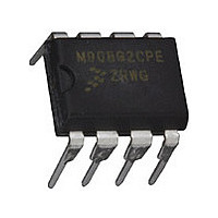
MC68HC908QT2CPE Freescale, MC68HC908QT2CPE Datasheet - Page 138

MC68HC908QT2CPE
Manufacturer Part Number
MC68HC908QT2CPE
Description
Manufacturer
Freescale
Datasheet
1.MC68HC908QT2CPE.pdf
(184 pages)
Specifications of MC68HC908QT2CPE
Cpu Family
HC08
Device Core Size
8b
Frequency (max)
8MHz
Total Internal Ram Size
128Byte
# I/os (max)
6
Number Of Timers - General Purpose
2
Operating Supply Voltage (typ)
3.3/5V
Operating Supply Voltage (max)
5.5V
Operating Supply Voltage (min)
2.7V
On-chip Adc
4-chx8-bit
Instruction Set Architecture
CISC
Operating Temp Range
-40C to 85C
Operating Temperature Classification
Industrial
Mounting
Through Hole
Pin Count
8
Package Type
PDIP
Program Memory Type
Flash
Program Memory Size
1.5KB
Lead Free Status / RoHS Status
Compliant
- Current page: 138 of 184
- Download datasheet (2Mb)
Development Support
15.2.2.5 Break Flag Control Register
The break control register (BFCR) contains a bit that enables software to clear status bits while the MCU
is in a break state.
BCFE — Break Clear Flag Enable Bit
15.2.3 Low-Power Modes
The WAIT and STOP instructions put the MCU in low power- consumption standby modes. If enabled,
the break module will remain enabled in wait and stop modes. However, since the internal address bus
does not increment in these modes, a break interrupt will never be triggered.
15.3 Monitor Module (MON)
This subsection describes the monitor module (MON) and the monitor mode entry methods. The monitor
allows debugging and programming of the microcontroller unit (MCU) through a single-wire interface with
a host computer. Monitor mode entry can be achieved without use of the higher test voltage, V
long as vector addresses $FFFE and $FFFF are blank, thus reducing the hardware requirements for
in-circuit programming.
Features include:
1. No security feature is absolutely secure. However, Freescale’s strategy is to make reading or copying the FLASH difficult for
138
unauthorized users.
This read/write bit enables software to clear status bits by accessing status registers while the MCU is
in a break state. To clear status bits during the break state, the BCFE bit must be set.
•
•
•
•
•
•
•
•
•
•
1 = Status bits clearable during break
0 = Status bits not clearable during break
Normal user-mode pin functionality on most pins
One pin dedicated to serial communication between MCU and host computer
Standard non-return-to-zero (NRZ) communication with host computer
Execution of code in random-access memory (RAM) or FLASH
FLASH memory security feature
FLASH memory programming interface
Use of external 9.8304 MHz oscillator to generate internal frequency of 2.4576 MHz
Simple internal oscillator mode of operation (no external clock or high voltage)
Monitor mode entry without high voltage, V
$FF)
Standard monitor mode entry if high voltage is applied to IRQ
Address: $FE03
Reset:
Read:
Write:
BCFE
Bit 7
R
0
Figure 15-8. Break Flag Control Register (BFCR)
= Reserved
MC68HC908QY/QT Family Data Sheet, Rev. 6
R
6
(1)
R
5
TST
R
4
, if reset vector is blank ($FFFE and $FFFF contain
R
3
R
2
R
1
Freescale Semiconductor
Bit 0
R
TST
, as
Related parts for MC68HC908QT2CPE
Image
Part Number
Description
Manufacturer
Datasheet
Request
R

Part Number:
Description:
TOWER ELEVATOR BOARDS HARDWARE
Manufacturer:
Freescale Semiconductor
Datasheet:

Part Number:
Description:
TOWER SERIAL I/O HARDWARE
Manufacturer:
Freescale Semiconductor
Datasheet:

Part Number:
Description:
LCD MODULE FOR TWR SYSTEM
Manufacturer:
Freescale Semiconductor
Datasheet:

Part Number:
Description:
DAUGHTER LCD WVGA I.MX51
Manufacturer:
Freescale Semiconductor
Datasheet:

Part Number:
Description:
TOWER SYSTEM BOARD MPC5125
Manufacturer:
Freescale Semiconductor
Datasheet:

Part Number:
Description:
KIT EVALUATION I.MX51
Manufacturer:
Freescale Semiconductor
Datasheet:

Part Number:
Description:
KIT DEVELOPMENT WINCE IMX25
Manufacturer:
Freescale Semiconductor
Datasheet:

Part Number:
Description:
TOWER SYSTEM KIT MPC5125
Manufacturer:
Freescale Semiconductor
Datasheet:

Part Number:
Description:
TOWER SYSTEM BOARD K40X256
Manufacturer:
Freescale Semiconductor
Datasheet:

Part Number:
Description:
TOWER SYSTEM KIT K40X256
Manufacturer:
Freescale Semiconductor
Datasheet:

Part Number:
Description:
Microcontrollers (MCU) MX28 PLATFORM DEV KIT
Manufacturer:
Freescale Semiconductor
Datasheet:

Part Number:
Description:
MCU, MPU & DSP Development Tools IAR KickStart Kit for Kinetis K60
Manufacturer:
Freescale Semiconductor
Datasheet:

Part Number:
Description:
24BIT HDMI MX535/08
Manufacturer:
Freescale Semiconductor
Datasheet:
Part Number:
Description:
Manufacturer:
Freescale Semiconductor, Inc
Datasheet:
Part Number:
Description:
Manufacturer:
Freescale Semiconductor, Inc
Datasheet:


