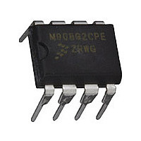
MC68HC908QT2CPE Freescale, MC68HC908QT2CPE Datasheet - Page 119

MC68HC908QT2CPE
Manufacturer Part Number
MC68HC908QT2CPE
Description
Manufacturer
Freescale
Datasheet
1.MC68HC908QT2CPE.pdf
(184 pages)
Specifications of MC68HC908QT2CPE
Cpu Family
HC08
Device Core Size
8b
Frequency (max)
8MHz
Total Internal Ram Size
128Byte
# I/os (max)
6
Number Of Timers - General Purpose
2
Operating Supply Voltage (typ)
3.3/5V
Operating Supply Voltage (max)
5.5V
Operating Supply Voltage (min)
2.7V
On-chip Adc
4-chx8-bit
Instruction Set Architecture
CISC
Operating Temp Range
-40C to 85C
Operating Temperature Classification
Industrial
Mounting
Through Hole
Pin Count
8
Package Type
PDIP
Program Memory Type
Flash
Program Memory Size
1.5KB
Lead Free Status / RoHS Status
Compliant
- Current page: 119 of 184
- Download datasheet (2Mb)
Chapter 14
Timer Interface Module (TIM)
14.1 Introduction
This section describes the timer interface module (TIM). The TIM is a two-channel timer that provides a
timing reference with input capture, output compare, and pulse-width-modulation functions.
is a block diagram of the TIM.
14.2 Features
Features of the TIM include the following:
14.3 Pin Name Conventions
The TIM shares two input/output (I/O) pins with two port A I/O pins. The full names of the TIM I/O pins are
listed in
Freescale Semiconductor
•
•
•
•
•
•
Two input capture/output compare channels
–
–
Buffered and unbuffered pulse width modulation (PWM) signal generation
Programmable TIM clock input
–
–
Free-running or modulo up-count operation
Toggle any channel pin on overflow
TIM counter stop and reset bits
Table
Rising-edge, falling-edge, or any-edge input capture trigger
Set, clear, or toggle output compare action
7-frequency internal bus clock prescaler selection
External TIM clock input
14-1. The generic pin name appear in the text that follows.
TIM Generic Pin Names:
Full TIM Pin Names:
MC68HC908QY/QT Family Data Sheet, Rev. 6
Table 14-1. Pin Name Conventions
PTA0/TCH0
TCH0
PTA1/TCH1
TCH1
PTA2/TCLK
TCLK
Figure 14-2
119
Related parts for MC68HC908QT2CPE
Image
Part Number
Description
Manufacturer
Datasheet
Request
R

Part Number:
Description:
TOWER ELEVATOR BOARDS HARDWARE
Manufacturer:
Freescale Semiconductor
Datasheet:

Part Number:
Description:
TOWER SERIAL I/O HARDWARE
Manufacturer:
Freescale Semiconductor
Datasheet:

Part Number:
Description:
LCD MODULE FOR TWR SYSTEM
Manufacturer:
Freescale Semiconductor
Datasheet:

Part Number:
Description:
DAUGHTER LCD WVGA I.MX51
Manufacturer:
Freescale Semiconductor
Datasheet:

Part Number:
Description:
TOWER SYSTEM BOARD MPC5125
Manufacturer:
Freescale Semiconductor
Datasheet:

Part Number:
Description:
KIT EVALUATION I.MX51
Manufacturer:
Freescale Semiconductor
Datasheet:

Part Number:
Description:
KIT DEVELOPMENT WINCE IMX25
Manufacturer:
Freescale Semiconductor
Datasheet:

Part Number:
Description:
TOWER SYSTEM KIT MPC5125
Manufacturer:
Freescale Semiconductor
Datasheet:

Part Number:
Description:
TOWER SYSTEM BOARD K40X256
Manufacturer:
Freescale Semiconductor
Datasheet:

Part Number:
Description:
TOWER SYSTEM KIT K40X256
Manufacturer:
Freescale Semiconductor
Datasheet:

Part Number:
Description:
Microcontrollers (MCU) MX28 PLATFORM DEV KIT
Manufacturer:
Freescale Semiconductor
Datasheet:

Part Number:
Description:
MCU, MPU & DSP Development Tools IAR KickStart Kit for Kinetis K60
Manufacturer:
Freescale Semiconductor
Datasheet:

Part Number:
Description:
24BIT HDMI MX535/08
Manufacturer:
Freescale Semiconductor
Datasheet:
Part Number:
Description:
Manufacturer:
Freescale Semiconductor, Inc
Datasheet:
Part Number:
Description:
Manufacturer:
Freescale Semiconductor, Inc
Datasheet:


