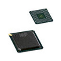
SAA7118E NXP Semiconductors, SAA7118E Datasheet - Page 62

SAA7118E
Manufacturer Part Number
SAA7118E
Description
Manufacturer
NXP Semiconductors
Datasheet
1.SAA7118E.pdf
(177 pages)
Specifications of SAA7118E
Adc/dac Resolution
9b
Screening Level
Commercial
Package Type
LBGA
Pin Count
156
Lead Free Status / RoHS Status
Compliant
Available stocks
Company
Part Number
Manufacturer
Quantity
Price
Part Number:
SAA7118E
Manufacturer:
PHILIPS/飞利浦
Quantity:
20 000
Company:
Part Number:
SAA7118E-V1
Manufacturer:
NXP
Quantity:
5 510
Company:
Part Number:
SAA7118E-V1
Manufacturer:
AD
Quantity:
5 510
Company:
Part Number:
SAA7118E/V1
Manufacturer:
PHI
Quantity:
480
Part Number:
SAA7118E/V1
Manufacturer:
PHILIPS/飞利浦
Quantity:
20 000
Company:
Part Number:
SAA7118E/V1,518
Manufacturer:
NXP Semiconductors
Quantity:
10 000
Company:
Part Number:
SAA7118E/V1,551
Manufacturer:
NXP Semiconductors
Quantity:
10 000
Company:
Part Number:
SAA7118E/V1,557
Manufacturer:
NXP Semiconductors
Quantity:
10 000
Part Number:
SAA7118E/V1/M5
Manufacturer:
PHILIPS/飞利浦
Quantity:
20 000
Company:
Part Number:
SAA7118E/V1/M5,518
Manufacturer:
Sigma Designs Inc
Quantity:
10 000
Company:
Part Number:
SAA7118EH
Manufacturer:
MNDSPEED
Quantity:
335
NXP Semiconductors
SAA7118_7
Product data sheet
8.6 Image port output formatter (subaddresses 84h to 87h)
Table 15.
[1]
The output interface consists of a FIFO for video and for sliced text data, an arbitration
circuit, which controls the mixed transfer of video and sliced text data over the I port and a
decoding and multiplexing unit, which generates the 8-bit or 16-bit wide output data
stream and the accompanied reference and supporting information.
The clock for the output interface can be derived from an internal clock, decoder,
expansion port, or an externally provided clock which is appropriate for e.g. VGA and
frame buffer. The clock can be up to 33 MHz. The scaler provides the following video
related timing reference events (signals), which are available on pins as defined by
subaddresses 84h and 85h:
The discontinuous data stream at the scaler output is accompanied by a data valid flag (or
data qualifier), or is transported via a gated clock. Clock cycles with invalid data on the
I port data bus (including the HPD pins in 16-bit output mode) are marked with code 00h.
The output interface also arbitrates the transfer between scaled video data and sliced text
data over the I port output.
The bits VITX1 and VITX0 (subaddress 86h) are used to control the arbitration.
As a further operation the serialization of the internal 32-bit double words to 8-bit or
optional 16-bit output, as well as the insertion of the extended ITU 656 codes (SAV/EAV
for video data, ANC or SAV/EAV codes for sliced text data) are done here.
For handshake with the VGA controller, or other memory or bus interface circuitry,
programmable FIFO flags are provided; see
DT[3:0]
62h[3:0]
1101
1110
1111
•
•
•
•
•
•
•
See errata information in
Output field ID
Start and end of vertical active video range
Start and end of active video line
Data qualifier or gated clock
Actually activated programming page (if CONLH is used)
Threshold controlled FIFO filling flags (empty, full and filled)
Sliced data marker
Standard type
MOJI (Japanese)
Japanese format switch
(L20/22)
no sliced data transmitted
(video data selected)
Data types supported by the data slicer block
Rev. 07 — 7 July 2008
Section
[1]
19.6.
Multistandard video decoder with adaptive comb filter
Data rate
(Mbit/s)
5.7272
5
5
Section
Framing Code
(FC)
programmable
(A7h)
programmable
none
8.6.2.
…continued
FC window Hamming
Japtext
open
disable
SAA7118
© NXP B.V. 2008. All rights reserved.
check
62 of 177


