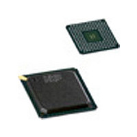
SAA7118E NXP Semiconductors, SAA7118E Datasheet - Page 33

SAA7118E
Manufacturer Part Number
SAA7118E
Description
Manufacturer
NXP Semiconductors
Datasheet
1.SAA7118E.pdf
(177 pages)
Specifications of SAA7118E
Adc/dac Resolution
9b
Screening Level
Commercial
Package Type
LBGA
Pin Count
156
Lead Free Status / RoHS Status
Compliant
Available stocks
Company
Part Number
Manufacturer
Quantity
Price
Part Number:
SAA7118E
Manufacturer:
PHILIPS/飞利浦
Quantity:
20 000
Company:
Part Number:
SAA7118E-V1
Manufacturer:
NXP
Quantity:
5 510
Company:
Part Number:
SAA7118E-V1
Manufacturer:
AD
Quantity:
5 510
Company:
Part Number:
SAA7118E/V1
Manufacturer:
PHI
Quantity:
480
Part Number:
SAA7118E/V1
Manufacturer:
PHILIPS/飞利浦
Quantity:
20 000
Company:
Part Number:
SAA7118E/V1,518
Manufacturer:
NXP Semiconductors
Quantity:
10 000
Company:
Part Number:
SAA7118E/V1,551
Manufacturer:
NXP Semiconductors
Quantity:
10 000
Company:
Part Number:
SAA7118E/V1,557
Manufacturer:
NXP Semiconductors
Quantity:
10 000
Part Number:
SAA7118E/V1/M5
Manufacturer:
PHILIPS/飞利浦
Quantity:
20 000
Company:
Part Number:
SAA7118E/V1/M5,518
Manufacturer:
Sigma Designs Inc
Quantity:
10 000
Company:
Part Number:
SAA7118EH
Manufacturer:
MNDSPEED
Quantity:
335
NXP Semiconductors
SAA7118_7
Product data sheet
8.1.3 Synchronization
8.1.4 Clock generation circuit
The prefiltered luminance signal is fed to the synchronization stage. Its bandwidth is
further reduced to 1 MHz in a low-pass filter. The sync pulses are sliced and fed to the
phase detectors where they are compared with the sub-divided clock frequency. The
resulting output signal is applied to the loop filter to accumulate all phase deviations.
Internal signals (e.g. HCL and HSY) are generated in accordance with analog front-end
requirements. The loop filter signal drives an oscillator to generate the Line Frequency
COntrol (LFCO) signal; see
The detection of ‘pseudo syncs’ as part of the Macrovision copy protection standard is
also achieved within the synchronization circuit.
The result is reported as flag COPRO within the decoder status byte at subaddress 1Fh.
The internal CGC generates all clock signals required for the video input processor.
The internal signal LFCO is a digital-to-analog converted signal provided by the horizontal
PLL. It is the multiple of the line frequency:
The LFCO signal is multiplied by a factor of 2 and 4 in the internal PLL circuit (including
phase detector, loop filtering, VCO and frequency divider) to obtain the output clock
signals. The rectangular output clocks have a 50 % duty factor.
Fig 20. CVBS (raw data) range for scaler input, data slicer and X port output
•
•
6.75 MHz = 429
6.75 MHz = 432
a. Sources containing 7.5 IRE black
255
209
71
CVBS levels with default settings RAWG[7:0] = 64 and RAWO[7:0] = 128.
Equation for modification of the raw data levels via bytes RAWG and RAWO:
It should be noted that the resulting levels are limited to 1 to 254 in accordance with “ITU
Recommendation 601/656” .
level offset (e.g. NTSC M).
60
CVBS
1
LUMINANCE
OUT
SYNC
=
Int
f
f
H
H
Rev. 07 — 7 July 2008
(50 Hz), or
(60 Hz)
RAWG
-----------------
black
black shoulder
sync bottom
white
64
Figure
001aac244
Multistandard video decoder with adaptive comb filter
CVBS
21.
nom
–
128
+
255
199
b. Sources not containing black level
60
RAWO
1
offset.
LUMINANCE
SYNC
white
black shoulder = black
sync bottom
SAA7118
© NXP B.V. 2008. All rights reserved.
001aac245
33 of 177


