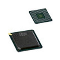
SAA7118E NXP Semiconductors, SAA7118E Datasheet - Page 131

SAA7118E
Manufacturer Part Number
SAA7118E
Description
Manufacturer
NXP Semiconductors
Datasheet
1.SAA7118E.pdf
(177 pages)
Specifications of SAA7118E
Adc/dac Resolution
9b
Screening Level
Commercial
Package Type
LBGA
Pin Count
156
Lead Free Status / RoHS Status
Compliant
Available stocks
Company
Part Number
Manufacturer
Quantity
Price
Part Number:
SAA7118E
Manufacturer:
PHILIPS/飞利浦
Quantity:
20 000
Company:
Part Number:
SAA7118E-V1
Manufacturer:
NXP
Quantity:
5 510
Company:
Part Number:
SAA7118E-V1
Manufacturer:
AD
Quantity:
5 510
Company:
Part Number:
SAA7118E/V1
Manufacturer:
PHI
Quantity:
480
Part Number:
SAA7118E/V1
Manufacturer:
PHILIPS/飞利浦
Quantity:
20 000
Company:
Part Number:
SAA7118E/V1,518
Manufacturer:
NXP Semiconductors
Quantity:
10 000
Company:
Part Number:
SAA7118E/V1,551
Manufacturer:
NXP Semiconductors
Quantity:
10 000
Company:
Part Number:
SAA7118E/V1,557
Manufacturer:
NXP Semiconductors
Quantity:
10 000
Part Number:
SAA7118E/V1/M5
Manufacturer:
PHILIPS/飞利浦
Quantity:
20 000
Company:
Part Number:
SAA7118E/V1/M5,518
Manufacturer:
Sigma Designs Inc
Quantity:
10 000
Company:
Part Number:
SAA7118EH
Manufacturer:
MNDSPEED
Quantity:
335
NXP Semiconductors
Table 102. I port FIFO flag control and arbitration; global set 86h[3:0]
[1]
Table 103. I port I/O enable, output clock and gated clock phase control; global set 87h[7:4]
[1]
[2]
Table 104. I port I/O enable, output clock and gated clock phase control; global set 87h[1:0]
SAA7118_7
Product data sheet
I port FIFO flag control and arbitration
FAE FIFO flag almost empty level
FAF FIFO flag almost full level
Output clock and gated clock phase control
ICLK default output phase
ICLK phase shifted by
ICKS0 = 0 (subaddress 80h)
ICLK phase shifted by approximately 3 ns
ICLK phase shifted by
3 ns
IDQ = gated clock default output phase
IDQ = gated clock phase shifted by
gated clock output
IDQ = gated clock phase shifted by approximately 3 ns
IDQ = gated clock phase shifted by
3 ns
I port I/O enable
I port output is disabled by software
I port output is enabled by software
I port output is enabled by pin ITRI at logic 0
I port output is enabled by pin ITRI at logic 1
< 16 double words
< 8 double words
< 4 double words
0 double words
32 double words
X = don’t care.
X = don’t care.
IPCK3 and IPCK2 only affect the gated clock (subaddress 80h, bit ICKS2 = 1).
16 double words
24 double words
28 double words
alternatively to setting ‘01’
alternatively to setting ‘01’
1
1
2
2
clock cycle
clock cycle + approximately
1
1
2
2
clock cycle
clock cycle + approximately
recommended for ICKS1 = 1 and
Rev. 07 — 7 July 2008
recommended for
Multistandard video decoder with adaptive comb filter
[1]
Control bits D3 to D0
FFL1
X
X
X
X
0
0
1
1
Control bits D7 to D4
IPCK3
X
X
X
X
0
0
1
1
Control bits D1 and D0
IPE1
0
0
1
1
[2]
FFL0
X
X
X
X
0
1
0
1
IPCK2
X
X
X
X
0
1
0
1
[2]
[1]
IPE0
0
1
0
1
FEL1
0
0
1
1
X
X
X
X
IPCK1
0
0
1
1
X
X
X
X
SAA7118
© NXP B.V. 2008. All rights reserved.
FEL0
0
1
0
1
X
X
X
X
IPCK0
0
1
0
1
X
X
X
X
131 of 177


