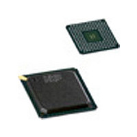
SAA7118E NXP Semiconductors, SAA7118E Datasheet - Page 166

SAA7118E
Manufacturer Part Number
SAA7118E
Description
Manufacturer
NXP Semiconductors
Datasheet
1.SAA7118E.pdf
(177 pages)
Specifications of SAA7118E
Adc/dac Resolution
9b
Screening Level
Commercial
Package Type
LBGA
Pin Count
156
Lead Free Status / RoHS Status
Compliant
Available stocks
Company
Part Number
Manufacturer
Quantity
Price
Part Number:
SAA7118E
Manufacturer:
PHILIPS/飞利浦
Quantity:
20 000
Company:
Part Number:
SAA7118E-V1
Manufacturer:
NXP
Quantity:
5 510
Company:
Part Number:
SAA7118E-V1
Manufacturer:
AD
Quantity:
5 510
Company:
Part Number:
SAA7118E/V1
Manufacturer:
PHI
Quantity:
480
Part Number:
SAA7118E/V1
Manufacturer:
PHILIPS/飞利浦
Quantity:
20 000
Company:
Part Number:
SAA7118E/V1,518
Manufacturer:
NXP Semiconductors
Quantity:
10 000
Company:
Part Number:
SAA7118E/V1,551
Manufacturer:
NXP Semiconductors
Quantity:
10 000
Company:
Part Number:
SAA7118E/V1,557
Manufacturer:
NXP Semiconductors
Quantity:
10 000
Part Number:
SAA7118E/V1/M5
Manufacturer:
PHILIPS/飞利浦
Quantity:
20 000
Company:
Part Number:
SAA7118E/V1/M5,518
Manufacturer:
Sigma Designs Inc
Quantity:
10 000
Company:
Part Number:
SAA7118EH
Manufacturer:
MNDSPEED
Quantity:
335
NXP Semiconductors
SAA7118_7
Product data sheet
19.2 Issue 2: Forced odd/even toggle option, enabled by bit FOET = 1
19.3 Issue 3: Errors with horizontal lock when using bit HLNRS (I
(I
properly
Background (how it should work):
Setting FOET = 1 is intended to make the odd/even output signal toggle fieldwise even if
the video source is of non-interlace type.
Anomaly description:
Although with a non-interlaced input the odd/even output signal toggles as desired, the
odd/even output signal might be just inverted (50 % likelihood), when the input signal is
changed to interlaced when FOET = 1.
Impact:
It cannot be assured that the generated odd/even sequence fits to the field sequence of
an interlaced input signal with activated FOET. Thus, in a succeeding processing, the two
field sequence of interlaced video could be swapped, resulting in a jaggy picture.
Workaround:
A continuous read on bit INTL (I
recognizes interlaced signals (FOET = 1 not allowed) and non-interlaced signals
(FOET = 1 is allowed) and FOET must be programmed depending on the state of INTL.
Alternatively, it always should be FOET = 0.
control signal, bit D6 of subaddress 03h)
Background (how it should work):
If horizontal lock is not possible because of very special input signals (like 250 kHz black
and white bars), HLNRS = 1 should enable to clamp to a mid range level (0.5 V) of the
input signal and a fast time constant AGC should increase signal amplitude to ADC input
range in order to force the horizontal PLL to lock. After horizontal PLL locking, AGC will be
switched to normal AGC time constant and a digitally controlled clamp circuit replaces the
‘clamp to a mid range level’ function automatically.
Anomaly description:
With HLNRS = 1, HOLDG = 0 and GAFIX = 0 in combination with unlocked horizontal
PLL, the video AGC is frozen to a small gain value.
Impact:
With gain reduced to a worst case minimum of 3 dB, it might happen that the digital sync
slicing threshold never is being reached and thus the horizontal PLL never gets locked.
Workaround:
HLNRS never should be set to logic 1 when the AGC is activated.
2
C-bus control signal, bit D5 of subaddress 08h) does not work
Rev. 07 — 7 July 2008
Multistandard video decoder with adaptive comb filter
2
C-bus control signal, bit D7 of subaddress 1Fh)
SAA7118
© NXP B.V. 2008. All rights reserved.
2
C-bus
166 of 177


