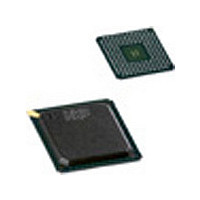
SAA7118E NXP Semiconductors, SAA7118E Datasheet - Page 151

SAA7118E
Manufacturer Part Number
SAA7118E
Description
Manufacturer
NXP Semiconductors
Datasheet
1.SAA7118E.pdf
(177 pages)
Specifications of SAA7118E
Adc/dac Resolution
9b
Screening Level
Commercial
Package Type
LBGA
Pin Count
156
Lead Free Status / RoHS Status
Compliant
Available stocks
Company
Part Number
Manufacturer
Quantity
Price
Part Number:
SAA7118E
Manufacturer:
PHILIPS/飞利浦
Quantity:
20 000
Company:
Part Number:
SAA7118E-V1
Manufacturer:
NXP
Quantity:
5 510
Company:
Part Number:
SAA7118E-V1
Manufacturer:
AD
Quantity:
5 510
Company:
Part Number:
SAA7118E/V1
Manufacturer:
PHI
Quantity:
480
Part Number:
SAA7118E/V1
Manufacturer:
PHILIPS/飞利浦
Quantity:
20 000
Company:
Part Number:
SAA7118E/V1,518
Manufacturer:
NXP Semiconductors
Quantity:
10 000
Company:
Part Number:
SAA7118E/V1,551
Manufacturer:
NXP Semiconductors
Quantity:
10 000
Company:
Part Number:
SAA7118E/V1,557
Manufacturer:
NXP Semiconductors
Quantity:
10 000
Part Number:
SAA7118E/V1/M5
Manufacturer:
PHILIPS/飞利浦
Quantity:
20 000
Company:
Part Number:
SAA7118E/V1/M5,518
Manufacturer:
Sigma Designs Inc
Quantity:
10 000
Company:
Part Number:
SAA7118EH
Manufacturer:
MNDSPEED
Quantity:
335
NXP Semiconductors
Table 147. Characteristics
V
levels refer to drawings and conditions illustrated in
SAA7118_7
Product data sheet
Symbol
9-bit analog-to-digital converters
B
G
f
LE
LE
Digital inputs
V
V
V
V
V
V
I
I
C
Digital outputs
V
V
V
clk(ADC)
LI
LI/O
DDD
diff
G
IL(SCL,SDA)
IH(SCL,SDA)
IL(XTALI)
IH(XTALI)
IL(n)
IH(n)
OL(SDA)
OL(clk)
OH(clk)
i
diff
dc(d)
dc(i)
ADC
= 3.0 V to 3.6 V; V
[4]
Parameter
analog bandwidth
differential phase
differential gain
ADC clock
frequency
DC differential
linearity error
DC integral linearity
error
ADC gain inequality
LOW-level input
voltage pins SDA
and SCL
HIGH-level input
voltage pins SDA
and SCL
LOW-level CMOS
input voltage pin
XTALI
HIGH-level CMOS
input voltage pin
XTALI
LOW-level input
voltage all other
inputs
HIGH-level input
voltage all other
inputs
input leakage
current
I/O leakage current
input capacitance
LOW-level output
voltage pin SDA
LOW-level output
voltage for clocks
HIGH-level output
voltage for clocks
DDA
= 3.1 V to 3.5 V; T
…continued
Conditions
at 3 dB
amplifier plus anti-alias filter
bypassed
amplifier plus anti-alias filter
bypassed
I/O at high-impedance
SDA at 3 mA sink current
maximum deviation
---------------------------------------------- - 1
minimum deviation
amb
= 0 C to 70 C (typical values measured at T
Figure
Rev. 07 — 7 July 2008
91; unless otherwise specified.
–
Multistandard video decoder with adaptive comb filter
100
[2]
[3]
[3]
Min
-
-
-
25.4
-
-
-
0.7V
2.0
2.0
-
-
-
-
0
2.4
0.5
0.3
0.3
DD(I2C)
Typ
7
2
2
-
0.7
1
3
-
-
-
-
-
-
-
-
-
-
-
-
amb
= 25 C); timings and
Max
-
-
-
28.6
-
-
-
+0.3V
V
+0.8
V
+0.8
5.5
1
10
8
0.4
0.6
V
SAA7118
© NXP B.V. 2008. All rights reserved.
DD(I2C)
DDD
DDD
+ 0.3
+ 0.5
DD(I2C)
+ 0.5 V
151 of 177
Unit
MHz
deg
%
MHz
LSB
LSB
%
V
V
V
V
V
pF
V
V
V
A
A


