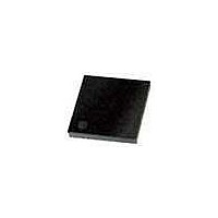
PIC18F43K20-E/MV Microchip Technology, PIC18F43K20-E/MV Datasheet - Page 397

PIC18F43K20-E/MV
Manufacturer Part Number
PIC18F43K20-E/MV
Description
8KB, Flash, 768bytes-RAM, 36I/O, 8-bit Family,nanowatt XLP 40 UQFN 5x5x0.5mm TUB
Manufacturer
Microchip Technology
Series
PIC® XLP™ 18Fr
Datasheet
1.PIC18F25K20T-ISS.pdf
(456 pages)
Specifications of PIC18F43K20-E/MV
Processor Series
PIC18
Core
PIC18F
Data Bus Width
8 bit
Program Memory Type
Flash
Program Memory Size
8 KB
Data Ram Size
512 B
Interface Type
I2C, SPI, SCI, USB, MSSP, RJ11
Maximum Clock Frequency
64 MHz
Number Of Programmable I/os
35
Number Of Timers
4
Operating Supply Voltage
1.8 V to 3.6 V
Maximum Operating Temperature
+ 125 C
Mounting Style
SMD/SMT
Package / Case
UQFN-40
Development Tools By Supplier
MPLAB Integrated Development Environment
Minimum Operating Temperature
- 40 C
Operating Temperature Range
- 40 C to + 125 C
Supply Current (max)
30 uA
Core Processor
PIC
Core Size
8-Bit
Speed
48MHz
Connectivity
I²C, SPI, UART/USART
Peripherals
Brown-out Detect/Reset, HLVD, POR, PWM, WDT
Number Of I /o
35
Eeprom Size
256 x 8
Ram Size
512 x 8
Voltage - Supply (vcc/vdd)
1.8 V ~ 3.6 V
Data Converters
A/D 14x10b
Oscillator Type
Internal
Operating Temperature
-40°C ~ 125°C
Lead Free Status / Rohs Status
Details
- Current page: 397 of 456
- Download datasheet (4Mb)
TABLE 26-19: I
2010 Microchip Technology Inc.
100
101
102
103
90
91
106
107
92
109
110
D102
Note 1:
Param.
No.
2:
Symbol
T
T
T
T
T
T
T
T
T
T
T
C
SU
SU
SU
AA
R
HIGH
LOW
F
HD
HD
BUF
B
As a transmitter, the device must provide this internal minimum delay time to bridge the undefined region
(min. 300 ns) of the falling edge of SCL to avoid unintended generation of Start or Stop conditions.
A fast mode I
T
LOW period of the SCL signal. If such a device does stretch the LOW period of the SCL signal, it must
output the next data bit to the SDA line, T
standard mode I
SU
:
:
:
:
:
STA
DAT
STO
STA
DAT
:
DAT
2
Clock High Time
Clock Low Time
SDA and SCL Rise
Time
SDA and SCL Fall
Time
Start Condition
Setup Time
Start Condition
Hold Time
Data Input Hold
Time
Data Input Setup
Time
Stop Condition
Setup Time
Output Valid from
Clock
Bus Free Time
Bus Capacitive Loading
C™ BUS DATA REQUIREMENTS (SLAVE MODE)
250 ns, must then be met. This will automatically be the case if the device does not stretch the
2
C bus device can be used in a standard mode I
2
C bus specification), before the SCL line is released.
Characteristic
100 kHz mode
400 kHz mode
SSP Module
100 kHz mode
400 kHz mode
SSP Module
100 kHz mode
400 kHz mode
100 kHz mode
400 kHz mode
100 kHz mode
400 kHz mode
100 kHz mode
400 kHz mode
100 kHz mode
400 kHz mode
100 kHz mode
400 kHz mode
100 kHz mode
400 kHz mode
100 kHz mode
400 kHz mode
100 kHz mode
400 kHz mode
R
max. + T
20 + 0.1 C
20 + 0.1 C
1.5 T
1.5 T
Min
250
100
4.0
0.6
4.7
1.3
4.7
0.6
4.0
0.6
4.7
0.6
4.7
1.3
—
—
—
—
—
SU
0
0
PIC18F2XK20/4XK20
CY
CY
:
DAT
B
B
= 1000 + 250 = 1250 ns (according to the
1000
3500
Max
2
300
300
300
0.9
400
—
—
—
—
—
—
—
—
—
—
—
—
—
—
—
—
—
—
C bus system but the requirement,
Units
pF
s
s
s
s
ns
ns
ns
ns
s
s
s
s
ns
s
ns
ns
s
s
ns
ns
s
s
PIC18FXXXX must operate
at a minimum of 1.5 MHz
PIC18FXXXX must operate
at a minimum of 10 MHz
PIC18FXXXX must operate
at a minimum of 1.5 MHz
PIC18FXXXX must operate
at a minimum of 10 MHz
C
10 to 400 pF
C
10 to 400 pF
Only relevant for Repeated
Start condition
After this period, the first
clock pulse is generated
(Note 2)
(Note 1)
Time the bus must be free
before a new transmission
can start
B
B
is specified to be from
is specified to be from
Conditions
DS41303G-page 397
Related parts for PIC18F43K20-E/MV
Image
Part Number
Description
Manufacturer
Datasheet
Request
R

Part Number:
Description:
Manufacturer:
Microchip Technology Inc.
Datasheet:

Part Number:
Description:
Manufacturer:
Microchip Technology Inc.
Datasheet:

Part Number:
Description:
Manufacturer:
Microchip Technology Inc.
Datasheet:

Part Number:
Description:
Manufacturer:
Microchip Technology Inc.
Datasheet:

Part Number:
Description:
Manufacturer:
Microchip Technology Inc.
Datasheet:

Part Number:
Description:
Manufacturer:
Microchip Technology Inc.
Datasheet:

Part Number:
Description:
Manufacturer:
Microchip Technology Inc.
Datasheet:

Part Number:
Description:
Manufacturer:
Microchip Technology Inc.
Datasheet:


