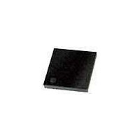
PIC18F43K20-E/MV Microchip Technology, PIC18F43K20-E/MV Datasheet - Page 150

PIC18F43K20-E/MV
Manufacturer Part Number
PIC18F43K20-E/MV
Description
8KB, Flash, 768bytes-RAM, 36I/O, 8-bit Family,nanowatt XLP 40 UQFN 5x5x0.5mm TUB
Manufacturer
Microchip Technology
Series
PIC® XLP™ 18Fr
Datasheet
1.PIC18F25K20T-ISS.pdf
(456 pages)
Specifications of PIC18F43K20-E/MV
Processor Series
PIC18
Core
PIC18F
Data Bus Width
8 bit
Program Memory Type
Flash
Program Memory Size
8 KB
Data Ram Size
512 B
Interface Type
I2C, SPI, SCI, USB, MSSP, RJ11
Maximum Clock Frequency
64 MHz
Number Of Programmable I/os
35
Number Of Timers
4
Operating Supply Voltage
1.8 V to 3.6 V
Maximum Operating Temperature
+ 125 C
Mounting Style
SMD/SMT
Package / Case
UQFN-40
Development Tools By Supplier
MPLAB Integrated Development Environment
Minimum Operating Temperature
- 40 C
Operating Temperature Range
- 40 C to + 125 C
Supply Current (max)
30 uA
Core Processor
PIC
Core Size
8-Bit
Speed
48MHz
Connectivity
I²C, SPI, UART/USART
Peripherals
Brown-out Detect/Reset, HLVD, POR, PWM, WDT
Number Of I /o
35
Eeprom Size
256 x 8
Ram Size
512 x 8
Voltage - Supply (vcc/vdd)
1.8 V ~ 3.6 V
Data Converters
A/D 14x10b
Oscillator Type
Internal
Operating Temperature
-40°C ~ 125°C
Lead Free Status / Rohs Status
Details
- Current page: 150 of 456
- Download datasheet (4Mb)
PIC18F2XK20/4XK20
11.4.1
The PWM period is specified by the PR2 register of
Timer2. The PWM period can be calculated using the
formula of Equation 11-1.
EQUATION 11-1:
When TMR2 is equal to PR2, the following three events
occur on the next increment cycle:
• TMR2 is cleared
• The CCPx pin is set. (Exception: If the PWM duty
• The PWM duty cycle is latched from CCPR
DS41303G-page 150
cycle = 0%, the pin will not be set.)
CCPR
Note:
Note: T
PWM Period
x
H.
PWM PERIOD
The Timer2 postscaler (see Section 14.1
“Timer2 Operation”) is not used in the
determination of the PWM frequency.
OSC
= 1/F
=
(TMR2 Prescale Value)
PWM PERIOD
OSC
PR2
.
+
1
4 T
OSC
x
L into
11.4.2
The PWM duty cycle is specified by writing a 10-bit
value to multiple registers: CCPR
DCxB<1:0> bits of the CCPxCON register. The
CCPR
bits of the CCPxCON register contain the two LSbs.
CCPR
register can be written to at any time. The duty cycle
value is not latched into CCPR
completes (i.e., a match between PR2 and TMR2
registers occurs). While using the PWM, the CCPR
register is read-only.
Equation 11-2 is used to calculate the PWM pulse
width.
Equation 11-3 is used to calculate the PWM duty cycle
ratio.
EQUATION 11-2:
EQUATION 11-3:
The CCPR
used to double buffer the PWM duty cycle. This double
buffering is essential for glitchless PWM operation.
The 8-bit timer TMR2 register is concatenated with
either the 2-bit internal system clock (F
the prescaler, to create the 10-bit time base. The system
clock is used if the Timer2 prescaler is set to 1:1.
When the 10-bit time base matches the CCPR
2-bit latch, then the CCPx pin is cleared (see
Figure 11-3).
Duty Cycle Ratio
x
x
Pulse Width
L contains the eight MSbs and the DCxB<1:0>
L and DCxB<1:0> bits of the CCPxCON
x
PWM DUTY CYCLE
H register and a 2-bit internal latch are
=
T
OSC
=
PULSE WIDTH
DUTY CYCLE RATIO
CCPRxL:DCxB<1:0>
2010 Microchip Technology Inc.
---------------------------------------------------------- -
CCPRxL:DCxB<1:0>
(TMR2 Prescale Value)
4 PR2
x
H until after the period
x
+
OSC
L register and
1
), or 2 bits of
x
H and
x
H
Related parts for PIC18F43K20-E/MV
Image
Part Number
Description
Manufacturer
Datasheet
Request
R

Part Number:
Description:
Manufacturer:
Microchip Technology Inc.
Datasheet:

Part Number:
Description:
Manufacturer:
Microchip Technology Inc.
Datasheet:

Part Number:
Description:
Manufacturer:
Microchip Technology Inc.
Datasheet:

Part Number:
Description:
Manufacturer:
Microchip Technology Inc.
Datasheet:

Part Number:
Description:
Manufacturer:
Microchip Technology Inc.
Datasheet:

Part Number:
Description:
Manufacturer:
Microchip Technology Inc.
Datasheet:

Part Number:
Description:
Manufacturer:
Microchip Technology Inc.
Datasheet:

Part Number:
Description:
Manufacturer:
Microchip Technology Inc.
Datasheet:


