MCP4728T-E/UN Microchip Technology, MCP4728T-E/UN Datasheet - Page 33
MCP4728T-E/UN
Manufacturer Part Number
MCP4728T-E/UN
Description
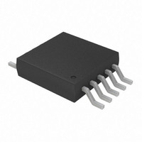
Quad, 12-bit NV DAC With I2C Interface 10 MSOP 3x3mm T/R
Manufacturer
Microchip Technology
Datasheet
1.MCP4728-EUN.pdf
(68 pages)
Specifications of MCP4728T-E/UN
Settling Time
6µs
Number Of Bits
12
Data Interface
I²C
Number Of Converters
4
Voltage Supply Source
Single Supply
Operating Temperature
-40°C ~ 125°C
Mounting Type
Surface Mount
Package / Case
10-MSOP, Micro10™, 10-uMAX, 10-uSOP
Lead Free Status / RoHS Status
Lead free / RoHS Compliant
For Use With
MCP4728EV - BOARD EVAL 12BIT 4CH DAC MCP4728
Power Dissipation (max)
-
Lead Free Status / RoHS Status
Lead free / RoHS Compliant
Available stocks
Company
Part Number
Manufacturer
Quantity
Price
Company:

Part Number:
MCP4728T-E/UN
Manufacturer:
MICROCHIP
Quantity:
12 000


5.4.4
This command is used to read the I
the device. If the second byte is “00001100” (0Ch), the
device will output its address bits stored in EEPROM
and register. This command uses the LDAC pin to
FIGURE 5-6:
© 2010 Microchip Technology Inc.
Start
S 0 0 0 0 0 0 0 0 A 0 0 0 0 1 1 0 0 A Sr 1 1 0 0 X X X 1 A A2 A1 A0 1 A2 A1 A0 0 A P
Clock Pulse
(CLK Line)
Clock and LDAC Transition Details:
LDAC Pin
Note 1: Clock Pulse and LDAC Transition Details.
(General Call Address)
LDAC Pin
2nd Byte
2:
3: LDAC pin resumes its normal function after “Stop” bit.
GENERAL CALL READ ADDRESS
BITS
1st Byte
6
LDAC pin events at the 2nd and 3rd bytes.
a.
b.
c.
Note 2 (a)
7
Keep LDAC pin “High” until the end of the positive pulse of the 8th clock of the 2nd byte.
LDAC pin makes a transition from “High” to “Low” during the negative pulse of the 8th clock of the 2nd
byte (just before the rising edge of the 9th clock) and stays “Low” until the rising edge of clock 9 of the
3rd byte.
The MCP4728 device does not acknowledge the 3rd byte if the conditions (a) and (b) are not met.
General Call Read I
ACK Clock
8
9
Note 2(b, c)
2
Sr
2nd Byte
C address bits of
Restart Clock
Stay “Low” until the end of the 3rd Byte
1
2
C Address.
ACK (MCP4728)
2
3
Note 2(b)
Restart
4
(Notes 1, 2, 3)
3rd Byte
select the device of interest to read on the I
LDAC pin needs a logic transition from “High” to “Low”
during the negative pulse of the 8th clock of the second
byte, and stays “Low” until the end of the 3rd byte. The
maximum clock rate for this command is 400 kHz.
Restart Byte
5
3rd Byte
6
7
8
Address Bits
EEPROM
ACK Clock
9
Reading Address Bits
in
4th Byte
Note 3
1
MCP4728
Reading Address Bits
Note 3
Address Bits
4th Byte
2
Register
in Input
DS22187E-page 33
ACK (Master)
3
2
C bus. The
Stop
Related parts for MCP4728T-E/UN
Image
Part Number
Description
Manufacturer
Datasheet
Request
R

Part Number:
Description:
IC DAC 12BIT W/I2C 10-MSOP
Manufacturer:
Microchip Technology
Datasheet:

Part Number:
Description:
12-bit, Quad Digital-to-analog Converter With Eeprom Memory
Manufacturer:
Microchip Technology Inc.
Datasheet:
Part Number:
Description:
Manufacturer:
Microchip Technology Inc.
Datasheet:
Part Number:
Description:
Manufacturer:
Microchip Technology Inc.
Datasheet:
Part Number:
Description:
Manufacturer:
Microchip Technology Inc.
Datasheet:
Part Number:
Description:
Manufacturer:
Microchip Technology Inc.
Datasheet:
Part Number:
Description:
Manufacturer:
Microchip Technology Inc.
Datasheet:
Part Number:
Description:
Manufacturer:
Microchip Technology Inc.
Datasheet:
Part Number:
Description:
Manufacturer:
Microchip Technology Inc.
Datasheet:
Part Number:
Description:
Manufacturer:
Microchip Technology Inc.
Datasheet: