MCP4728T-E/UN Microchip Technology, MCP4728T-E/UN Datasheet - Page 21
MCP4728T-E/UN
Manufacturer Part Number
MCP4728T-E/UN
Description
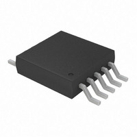
Quad, 12-bit NV DAC With I2C Interface 10 MSOP 3x3mm T/R
Manufacturer
Microchip Technology
Datasheet
1.MCP4728-EUN.pdf
(68 pages)
Specifications of MCP4728T-E/UN
Settling Time
6µs
Number Of Bits
12
Data Interface
I²C
Number Of Converters
4
Voltage Supply Source
Single Supply
Operating Temperature
-40°C ~ 125°C
Mounting Type
Surface Mount
Package / Case
10-MSOP, Micro10™, 10-uMAX, 10-uSOP
Lead Free Status / RoHS Status
Lead free / RoHS Compliant
For Use With
MCP4728EV - BOARD EVAL 12BIT 4CH DAC MCP4728
Power Dissipation (max)
-
Lead Free Status / RoHS Status
Lead free / RoHS Compliant
Available stocks
Company
Part Number
Manufacturer
Quantity
Price
Company:

Part Number:
MCP4728T-E/UN
Manufacturer:
MICROCHIP
Quantity:
12 000


3.0
The descriptions of the pins are listed in
TABLE 3-1:
3.1
V
at the V
as a DAC external reference. The power supply at the
V
performance.
It is recommended to use an appropriate bypass
capacitor of about 0.1 µF (ceramic) to ground. An
additional 10 µF capacitor (tantalum) in parallel is also
recommended to further attenuate high-frequency
noise present in application boards. The supply voltage
(V
specified operation.
V
device. The user must connect the V
plane through a low-impedance connection. If an
analog ground path is available in the application
printed circuit board (PCB), it is highly recommended
that the V
isolated within an analog ground plane of the circuit
board.
© 2010 Microchip Technology Inc.
Legend: P = Power, OI = Open-Drain Input, OO = Open-Drain Output, ST = Schmitt Trigger Input Buffer,
Note 1:
Pin No.
DD
DD
SS
DD
10
1
2
3
4
5
6
7
8
9
is the ground pin and the current return path of the
is the power supply pin for the device. The voltage
pin should be as clean as possible for a good DAC
) must be maintained in the 2.7V to 5.5V range for
2:
DD
PIN DESCRIPTIONS
Supply Voltage Pins (V
SS
AO = Analog Output
RDY/BSY
pin is used as a power supply input as well
This pin needs an external pull-up resistor from V
This pin can be driven by MCU.
V
V
V
V
Name
LDAC
pin be tied to the analog ground path, or
SDA
OUT
OUT
SCL
OUT
OUT
V
V
DD
SS
PIN FUNCTION TABLE
A
C
D
B
Pin Type
OI/OO
OO
AO
AO
AO
AO
ST
OI
P
P
Supply Voltage
I
I
This pin is used for two purposes:
(a) Synchronization Input. It is used to transfer the contents of the DAC input
registers to the output registers (V
(b) Select the device for reading and writing I
This pin is a status indicator of EEPROM programming activity. An external pull-up
resistor (about 100 kΩ) is needed from RDY/BSY pin to V
Buffered analog voltage output of channel A. The output amplifier has rail-to-rail
operation.
Buffered analog voltage output of channel B. The output amplifier has rail-to-rail
operation.
Buffered analog voltage output of channel C. The output amplifier has rail-to-rail
operation.
Buffered analog voltage output of channel D. The output amplifier has rail-to-rail
operation.
Ground reference.
2
2
C Serial Clock Input
C Serial Data Input and Output
SS
DD
pin to a ground
Table
, V
SS
3-1.
)
(Note
DD
1)
3.2
SCL is the serial clock pin of the I
MCP4728 device acts only as a slave and the SCL pin
accepts only external input serial clocks. The input data
from the Master device is shifted into the SDA pin on
the rising edges of the SCL clock, and output from the
MCP4728 occurs at the falling edges of the SCL clock.
The SCL pin is an open-drain N-channel driver.
Therefore, it needs a pull-up resistor from the V
to the SCL pin.
Refer
Communications”
Interface communication.
Typical range of the pull-up resistor value for SCL and
SDA is from 5 kΩ to 10 kΩ for Standard (100 kHz) and
Fast (400 kHz) modes, and less than 1 kΩ for High
Speed mode (3.4 MHz).
line. Leave this pin float if it is not used.
(Note
OUT
Function
).
to
Serial Clock Pin (SCL)
1)
Section 5.0
2
C address bits.
for more details on I
DD
“I
MCP4728
2
line.
C
(Note
(Note
Serial
2
DS22187E-page 21
C interface. The
2)
1)
2
Interface
C Serial
DD
line
Related parts for MCP4728T-E/UN
Image
Part Number
Description
Manufacturer
Datasheet
Request
R

Part Number:
Description:
IC DAC 12BIT W/I2C 10-MSOP
Manufacturer:
Microchip Technology
Datasheet:

Part Number:
Description:
12-bit, Quad Digital-to-analog Converter With Eeprom Memory
Manufacturer:
Microchip Technology Inc.
Datasheet:
Part Number:
Description:
Manufacturer:
Microchip Technology Inc.
Datasheet:
Part Number:
Description:
Manufacturer:
Microchip Technology Inc.
Datasheet:
Part Number:
Description:
Manufacturer:
Microchip Technology Inc.
Datasheet:
Part Number:
Description:
Manufacturer:
Microchip Technology Inc.
Datasheet:
Part Number:
Description:
Manufacturer:
Microchip Technology Inc.
Datasheet:
Part Number:
Description:
Manufacturer:
Microchip Technology Inc.
Datasheet:
Part Number:
Description:
Manufacturer:
Microchip Technology Inc.
Datasheet:
Part Number:
Description:
Manufacturer:
Microchip Technology Inc.
Datasheet: