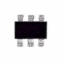
NDC652P Fairchild Semiconductor, NDC652P Datasheet

NDC652P
Specifications of NDC652P
Available stocks
Related parts for NDC652P
NDC652P Summary of contents
Page 1
... High density cell design for extremely low R Exceptional on-resistance and maximum DC current capability 25°C unless otherwise noted A (Note 1a) (Note 1b) (Note 1c) ) (Note 1a (Note 1) March 1996 = 0. -4.5V DS(ON 0. -10V. DS(ON package design using copper . DS(ON NDC652P Units -30 -20 -2.4 -10 1.6 1 0.8 -55 to 150 78 °C/W 30 °C/W NDC652P Rev °C ...
Page 2
... A Conditions -250 µ - - -250 µ - 1.0 MHz GEN GEN Min Typ Max - 100 -100 -1 -1 125 C -0.7 -1.2 -2.2 J 0.16 0. 125 C 0.22 0.36 J 0.09 0. 290 180 10.5 20 1.5 3.3 NDC652P Rev. D1 Units V µA µ ...
Page 3
... C/W when mounted on a 0.003 in pad of 2oz cpper. 1a Scale letter size paper 2. Pulse Test: Pulse Width < 300µs, Duty Cycle < 2.0%. = 25°C unless otherwise noted) A Conditions -1.3 A (Note Min Typ Max Units -1.3 -0.8 -1.2 is guaranteed NDC652P Rev ...
Page 4
... GS -3.5 -4.0 -4.5 -5 DRAIN CURRENT (A) D Figure 2. On-Resistance Variation 125°C J 25°C -55° DRAIN CURRENT (A) D Figure 4. On-Resistance Variation -250µ JUNCTION TEMPERATURE (°C) J Figure 6. Gate Threshold Variation with Temperature -5.5 -6.0 -7.0 -10 -10 - NDC652P Rev. D1 ...
Page 5
... C rss Figure 10. Gate Charge Characteristics t d(on OUT 125°C J 25°C -55°C 0.4 0.6 0 BODY DIODE FORWARD VOLTAGE (V) SD Source Current and Temperature V = -5V = -2.4A DS -15V -10V GATE CHARGE (nC off t t d(off PULSE WIDTH Figure 12. Switching Waveforms 1 INVERTED NDC652P Rev. D1 ...
Page 6
... Figure 16. Maximum Safe Operating Area 0.001 0.01 0 TIME (sec 4.5"x5" FR-4 Board Still Air 0.2 0.4 0.6 0.8 2 2oz COPPER MOUNTING PAD AREA ( -4.5V GS SINGLE PULSE = See Note 25° DRAIN-SOURCE VOLTAGE ( ( See Note 1c JA P(pk ( Duty Cycle 100 300 NDC652P Rev. D1 ...
Page 7
... Pizza Box fo r Standar d Opti on SSOT-6 Tape Leader and Trailer Configuration: Figur e 2.0 Carrier Tape Cover Tape Traile r Tape 300mm mi nimum or 75 empty poc kets 1998 Fairchild Semiconductor Corporation Anti static Cover Tape Embossed F63TNR Carrier Tape Label 631 631 SSOT-6 Unit Orientation ...
Page 8
SuperSOT TM -6 Tape and Reel Data and Package Dimensions, continued SSOT-6 Embossed Carrier Tape Configuration: Figure 3 Pkg type SSOT-6 3.23 3.18 8.0 1.55 +/-0.10 +/-0.10 +/-0.3 +/-0.05 (8mm) Notes: ...
Page 9
... SuperSOT TM -6 Tape and Reel Data and Package Dimensions, continued SuperSOT -6 (FS PKG Code 31, 33) 1998 Fairchild Semiconductor Corporation 1:1 Scale 1:1 on letter size paper Dimensions shown below are in: inches [millimeters] Part Weight per unit (gram): 0.0158 September 1998, Rev. A ...
Page 10
... TRADEMARKS The following are registered and unregistered trademarks Fairchild Semiconductor owns or is authorized to use and is not intended exhaustive list of all such trademarks. ACEx™ CoolFET™ CROSSVOLT™ CMOS FACT™ FACT Quiet Series™ ® FAST FASTr™ GTO™ ...


