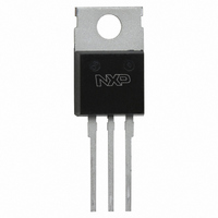
BUK9504-40A,127 NXP Semiconductors, BUK9504-40A,127 Datasheet - Page 5

BUK9504-40A,127
Manufacturer Part Number
BUK9504-40A,127
Description
MOSFET N-CH 40V 75A SOT78
Manufacturer
NXP Semiconductors
Series
TrenchMOS™r
Datasheet
1.BUK9E04-40A127.pdf
(15 pages)
Specifications of BUK9504-40A,127
Fet Type
MOSFET N-Channel, Metal Oxide
Fet Feature
Logic Level Gate
Rds On (max) @ Id, Vgs
4 mOhm @ 25A, 10V
Drain To Source Voltage (vdss)
40V
Current - Continuous Drain (id) @ 25° C
75A
Vgs(th) (max) @ Id
2V @ 1mA
Gate Charge (qg) @ Vgs
128nC @ 5V
Input Capacitance (ciss) @ Vds
8260pF @ 25V
Power - Max
300W
Mounting Type
Through Hole
Package / Case
TO-220AB-3
Configuration
Single
Transistor Polarity
N-Channel
Resistance Drain-source Rds (on)
0.004 Ohms
Drain-source Breakdown Voltage
40 V
Gate-source Breakdown Voltage
+/- 15 V
Continuous Drain Current
198 A
Power Dissipation
300 W
Maximum Operating Temperature
+ 175 C
Mounting Style
Through Hole
Minimum Operating Temperature
- 55 C
Lead Free Status / RoHS Status
Lead free / RoHS Compliant
Other names
934056692127
BUK9504-40A
BUK9504-40A
BUK9504-40A
BUK9504-40A
Philips Semiconductors
8. Characteristics
Table 5:
T
9397 750 08649
Product data
Symbol
Static characteristics
V
V
I
I
R
Dynamic characteristics
Q
Q
Q
C
C
C
t
t
t
t
L
L
DSS
GSS
d(on)
r
d(off)
f
j
d
s
(BR)DSS
GS(th)
DSon
iss
oss
rss
g(tot)
gs
gd
= 25 C unless otherwise specified
Characteristics
Parameter
drain-source breakdown
voltage
gate-source threshold voltage I
drain-source leakage current
gate-source leakage current
drain-source on-state
resistance
total gate charge
gate-to-source charge
gate-to-drain (Miller) charge
input capacitance
output capacitance
reverse transfer capacitance
turn-on delay time
rise time
turn-off delay time
fall time
internal drain inductance
internal source inductance
Conditions
I
Figure 9
V
V
V
Figure 7
V
V
V
I
V
f = 1 MHz;
V
V
from drain lead 6 mm from
package to centre of die
from contact screw on
mounting base to centre of
die SOT78
from upper edge of drain
mounting base to centre of
die SOT404 / SOT226
from source lead to source
bond pad
D
D
D
DS
GS
GS
GS
GS
GS
GS
DD
GS
T
T
T
T
T
T
T
T
T
= 0.25 mA; V
= 1 mA; V
= 25 A;
j
j
j
j
j
j
j
j
j
= 40 V; V
= 25 C
= 55 C
= 25 C
= 175 C
= 55 C
= 25 C
= 175 C
= 10 V; V
= 5 V; I
= 25 C
= 175 C
= 4.3 V; I
= 10 V; I
= 5 V; V
= 0 V; V
= 30 V; R
= 5 V; R
Rev. 01 — 24 October 2001
and
Figure 14
Figure 12
D
DS
DD
DS
G
D
8
= 25 A;
D
GS
L
= 10
= 25 A
DS
= V
= 25 A
GS
= 32 V;
= 25 V;
= 1.2 ;
= 0 V
= 0 V
= 0 V
GS
;
BUK95/96/9E04-40A
Min
40
36
1
0.5
-
-
-
-
-
-
-
-
-
-
-
-
-
-
-
-
-
-
-
-
-
-
TrenchMOS™ logic level FET
© Koninklijke Philips Electronics N.V. 2001. All rights reserved.
Typ
-
-
1.5
-
-
0.05
-
2
3.5
-
3.7
2.9
128
13
56
6200
1040
680
62
309
365
306
4.5
3.5
2.5
7.5
Max
-
-
2
-
2.3
10
500
100
4.4
8.3
5.9
4
-
-
-
8260
1250
940
-
-
-
-
-
-
-
-
Unit
V
V
V
V
V
nA
m
m
m
m
nC
nC
nC
pF
pF
pF
ns
ns
ns
ns
nH
nH
nH
nH
5 of 15
A
A


