FDB8896 Fairchild Semiconductor, FDB8896 Datasheet - Page 2
FDB8896
Manufacturer Part Number
FDB8896
Description
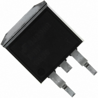
MOSFET N-CH 30V 93A TO-263AB
Manufacturer
Fairchild Semiconductor
Series
PowerTrench®r
Datasheet
1.FDB8896.pdf
(11 pages)
Specifications of FDB8896
Fet Type
MOSFET N-Channel, Metal Oxide
Fet Feature
Logic Level Gate
Rds On (max) @ Id, Vgs
5.7 mOhm @ 35A, 10V
Drain To Source Voltage (vdss)
30V
Current - Continuous Drain (id) @ 25° C
93A
Vgs(th) (max) @ Id
2.5V @ 250µA
Gate Charge (qg) @ Vgs
67nC @ 10V
Input Capacitance (ciss) @ Vds
2525pF @ 15V
Power - Max
80W
Mounting Type
Surface Mount
Package / Case
D²Pak, TO-263 (2 leads + tab)
Configuration
Single
Transistor Polarity
N-Channel
Resistance Drain-source Rds (on)
0.0057 Ohm @ 10 V
Drain-source Breakdown Voltage
30 V
Gate-source Breakdown Voltage
+/- 20 V
Continuous Drain Current
19 A
Power Dissipation
80000 mW
Maximum Operating Temperature
+ 175 C
Mounting Style
SMD/SMT
Minimum Operating Temperature
- 55 C
Lead Free Status / RoHS Status
Lead free / RoHS Compliant
Other names
FDB8896
FDB8896TR
FDB8896TR
Available stocks
Company
Part Number
Manufacturer
Quantity
Price
Company:

Part Number:
FDB8896
Manufacturer:
FSC
Quantity:
5 600
Company:
Part Number:
FDB8896
Manufacturer:
FSC
Quantity:
15 000
Part Number:
FDB8896
Manufacturer:
FAIRCHILD/仙童
Quantity:
20 000


©2008 Fairchild Semiconductor Corporation
Electrical Characteristics
Off Characteristics
On Characteristics
Dynamic Characteristics
Switching Characteristics
Drain-Source Diode Characteristics
Notes:
1: Package current limitation is 80A.
2: Starting T
3: Pulse width = 100s.
4
B
I
I
V
r
C
C
C
R
Q
Q
Q
Q
Q
Q
t
t
t
t
t
t
V
t
Q
DSS
GSS
ON
d(ON)
r
d(OFF)
f
OFF
rr
DS(ON)
GS(TH)
VDSS
SD
ISS
OSS
RSS
G
g(TOT)
g(5)
g(TH)
gs
gs2
gd
RR
Symbol
J
= 25°C, L = 36 H, I
Drain to Source Breakdown Voltage
Zero Gate Voltage Drain Current
Gate to Source Leakage Current
Gate to Source Threshold Voltage
Drain to Source On Resistance
Input Capacitance
Output Capacitance
Reverse Transfer Capacitance
Gate Resistance
Total Gate Charge at 10V
Total Gate Charge at 5V
Threshold Gate Charge
Gate to Source Gate Charge
Gate Charge Threshold to Plateau
Gate to Drain “Miller” Charge
Turn-On Time
Turn-On Delay Time
Rise Time
Turn-Off Delay Time
Fall Time
Turn-Off Time
Source to Drain Diode Voltage
Reverse Recovery Time
Reverse Recovered Charge
AS
= 64A, V
Parameter
DD
(V
= 27V, V
GS
= 10V)
T
C
GS
= 25°C unless otherwise noted
= 10V.
V
V
V
I
I
V
V
V
I
I
I
T
V
f = 1MHz
V
V
V
V
I
I
I
D
D
D
D
SD
SD
SD
SD
J
DS
GS
GS
GS
DS
GS
GS
GS
GS
DD
GS
= 250 A, V
= 35A, V
= 35A, V
= 35A, V
= 175
= 35A
= 20A
= 35A, dI
= 35A, dI
= 24V
= 0V
= 20V
= V
= 15V, V
= 0.5V, f = 1MHz
= 0V to 10V
= 0V to 5V
= 0V to 1V
= 15V, I
= 4.5V, R
Test Conditions
DS
o
C
, I
GS
GS
GS
D
D
SD
SD
GS
GS
= 35A
GS
= 10V
= 4.5V
= 10V,
= 250 A
/dt = 100A/ s
/dt = 100A/ s
= 0V,
= 0V
= 6.2
T
V
I
I
D
g
C
DD
= 1.0mA
= 35A
= 150
= 15V
o
C
Min
1.2
30
-
-
-
-
-
-
-
-
-
-
-
-
-
-
-
-
-
-
-
-
-
-
-
-
-
-
0.0049 0.0057
0.0059 0.0068
0.0078 0.0094
2525
490
300
102
Typ
2.3
2.3
5.7
9.5
48
25
58
44
8
9
-
-
-
-
-
-
-
-
-
-
-
1.25
Max
250
167
153
2.5
3.0
1.0
100
67
36
27
12
1
-
-
-
-
-
-
-
-
-
-
-
-
FDB8896 Rev. B2
Units
nC
nC
nC
nC
nC
nC
nC
nA
pF
pF
pF
ns
ns
ns
ns
ns
ns
ns
V
V
V
V
A
Related parts for FDB8896
Image
Part Number
Description
Manufacturer
Datasheet
Request
R

Part Number:
Description:
Fairchild Semiconductor [IGBT MODULE]
Manufacturer:
Fairchild Semiconductor
Datasheet:

Part Number:
Description:
Discrete Semiconductor Modules
Manufacturer:
Fairchild Semiconductor
Part Number:
Description:
Discrete Semiconductor Modules
Manufacturer:
Fairchild Semiconductor
Part Number:
Description:
This N-Channel MOSFET is produced using Fairchild Semiconductor’s advanced Power Trench® process
Manufacturer:
Fairchild Semiconductor
Datasheet:
Part Number:
Description:
This N-Channel MOSFET is produced using Fairchild Semiconductor’s advanced Power Trench® process
Manufacturer:
Fairchild Semiconductor
Datasheet:
Part Number:
Description:
This N-Channel MOSFET is produced using Fairchild Semiconductor’s advanced PowerTrench® process
Manufacturer:
Fairchild Semiconductor
Datasheet:
Part Number:
Description:
This N-Channel MOSFET is produced using Fairchild Semiconductor’s advanced PowerTrench® process
Manufacturer:
Fairchild Semiconductor
Datasheet:
Part Number:
Description:
This N-Channel MOSFET is produced using Fairchild Semiconductor’s advanced Power Trench® process
Manufacturer:
Fairchild Semiconductor
Datasheet:
Part Number:
Description:
This N-Channel logic Level MOSFETs are produced using Fairchild Semiconductor‘s advanced Power Trench® process that has been special tailored to minimize the on-state resistance and yet maintain superior switching performance
Manufacturer:
Fairchild Semiconductor
Datasheet:
Part Number:
Description:
This N-Channel MOSFET is produced using Fairchild Semiconductor’s advanced Power Trench® process
Manufacturer:
Fairchild Semiconductor
Datasheet:
Part Number:
Description:
This N-Channel SyncFET™ is produced using Fairchild Semiconductor’s advanced PowerTrench® process
Manufacturer:
Fairchild Semiconductor
Datasheet:
Part Number:
Description:
This N-Channel SyncFET™ is produced using Fairchild Semiconductor’s advanced PowerTrench® process
Manufacturer:
Fairchild Semiconductor
Datasheet:
Part Number:
Description:
This N-Channel SyncFET™ is produced using Fairchild Semiconductor’s advanced PowerTrench® process
Manufacturer:
Fairchild Semiconductor
Datasheet:
Part Number:
Description:
This N-Channel logic Level MOSFETs are produced using Fairchild Semiconductor‘s advanced Power Trench® process that has been special tailored to minimize the on-state resistance and yet maintain superior switching performance
Manufacturer:
Fairchild Semiconductor
Datasheet:
Part Number:
Description:
This N-Channel MOSFET is produced using Fairchild Semiconductor’s advanced Power Trench® process that has been especially tailored to minimize the on-state resistance and yet maintain superior switching performance
Manufacturer:
Fairchild Semiconductor
Datasheet: