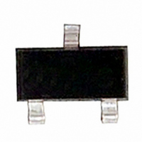
FDN352AP Fairchild Semiconductor, FDN352AP Datasheet - Page 4

FDN352AP
Manufacturer Part Number
FDN352AP
Description
MOSFET P-CH 30V 1.3A SSOT-3
Manufacturer
Fairchild Semiconductor
Series
PowerTrench®r
Datasheet
1.FDN352AP.pdf
(5 pages)
Specifications of FDN352AP
Fet Type
MOSFET P-Channel, Metal Oxide
Fet Feature
Logic Level Gate
Rds On (max) @ Id, Vgs
180 mOhm @ 1.3A, 10V
Drain To Source Voltage (vdss)
30V
Current - Continuous Drain (id) @ 25° C
1.3A
Vgs(th) (max) @ Id
2.5V @ 250µA
Gate Charge (qg) @ Vgs
1.9nC @ 4.5V
Input Capacitance (ciss) @ Vds
150pF @ 15V
Power - Max
460mW
Mounting Type
Surface Mount
Package / Case
3-SSOT, SuperSOT-3
Configuration
Single
Transistor Polarity
P-Channel
Resistance Drain-source Rds (on)
0.18 Ohm @ 10 V
Forward Transconductance Gfs (max / Min)
2 S
Drain-source Breakdown Voltage
30 V
Gate-source Breakdown Voltage
+/- 25 V
Continuous Drain Current
1.3 A
Power Dissipation
500 mW
Maximum Operating Temperature
+ 150 C
Mounting Style
SMD/SMT
Minimum Operating Temperature
- 55 C
Lead Free Status / RoHS Status
Lead free / RoHS Compliant
Other names
FDN352AP
Available stocks
Company
Part Number
Manufacturer
Quantity
Price
Company:
Part Number:
FDN352AP
Manufacturer:
FSC
Quantity:
69 000
Company:
Part Number:
FDN352AP
Manufacturer:
Intersil
Quantity:
130
Part Number:
FDN352AP
Manufacturer:
FAIRCHILD/仙童
Quantity:
20 000
Part Number:
FDN352AP-NL
Manufacturer:
ON/安森美
Quantity:
20 000
FDN352AP Rev. C1
Typical Characteristics
0.01
10
100
0.1
8
6
4
2
0
10
1
Figure 9. Maximum Safe Operating Area.
0
0.1
Figure 7. Gate Charge Characteristics.
I
D
= -0.9A
SINGLE PULSE
0.001
R
0.01
θ
V
JA
0.1
R
T
GS
DS(ON)
A
0.0001
1
= 270
= 25
0.5
= -10V
LIMIT
o
o
C
C/W
-V
D = 0.5
0.2
DS
0.1
0.05
0.02
, DRAIN-SOURCE VOLTAGE (V)
0.01
Q
1
1
g
, GATE CHARGE (nC)
SINGLE PULSE
V
0.001
DS
= -10V
Thermal characterization performed using the conditions described in Note 1c.
Transient thermal response will change depending on the circuit board design.
DC
1.5
10s
Figure 11. Transient Thermal Response Curve.
1s
-15V
100ms
10ms
2
10
1ms
0.01
-20V
100µs
2.5
100
3
0.1
t
1
4
, TIME (sec)
200
150
100
50
50
40
30
20
10
0.0001
0
0
0
Figure 8. Capacitance Characteristics.
C
1
rss
Figure 10. Single Pulse Maximum
0.001
5
-V
DS
Power Dissipation.
0.01
C
, DRAIN TO SOURCE VOLTAGE (V)
oss
10
10
t
0.1
1
, TIME (sec)
15
P(pk)
Duty Cycle, D = t
T
1
R
R
J
θ JA
– T
C
θ JA
100
iss
(t) = r(t) * R
A
t
= 270°C/W
1
20
= P * R
t
2
10
SINGLE PULSE
R
θ
JA
T
A
θ JA
= 270°C/W
= 25°C
θ JA
1
www.fairchildsemi.com
(t)
/ t
100
25
2
f = 1 MHz
V
GS
1000
= 0 V
1000
30


