FDN352AP Fairchild Semiconductor, FDN352AP Datasheet
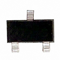
MOSFET P-CH 30V 1.3A SSOT-3

FDN352AP

Manufacturer Part Number
FDN352AP
Description
MOSFET P-CH 30V 1.3A SSOT-3
Manufacturer
Fairchild Semiconductor
Series
PowerTrench®r
Datasheet

Specifications of FDN352AP

Fet Type
MOSFET P-Channel, Metal Oxide
Fet Feature
Logic Level Gate
Rds On (max) @ Id, Vgs
180 mOhm @ 1.3A, 10V
Drain To Source Voltage (vdss)
30V
Current - Continuous Drain (id) @ 25° C
1.3A
Vgs(th) (max) @ Id
2.5V @ 250µA
Gate Charge (qg) @ Vgs
1.9nC @ 4.5V
Input Capacitance (ciss) @ Vds
150pF @ 15V
Power - Max
460mW
Mounting Type
Surface Mount
Package / Case
3-SSOT, SuperSOT-3
Configuration
Single
Transistor Polarity
P-Channel
Resistance Drain-source Rds (on)
0.18 Ohm @ 10 V
Forward Transconductance Gfs (max / Min)
2 S
Drain-source Breakdown Voltage
30 V
Gate-source Breakdown Voltage
+/- 25 V
Continuous Drain Current
1.3 A
Power Dissipation
500 mW
Maximum Operating Temperature
+ 150 C
Mounting Style
SMD/SMT
Minimum Operating Temperature
- 55 C
Lead Free Status / RoHS Status
Lead free / RoHS Compliant
Other names
FDN352AP

Available stocks

Company
Part Number
Manufacturer
Quantity
Price
Part Number:
FDN352AP
Manufacturer:
FSC
Quantity:
69 000
Part Number:
FDN352AP
Manufacturer:
Intersil
Quantity:
130
Part Number:
FDN352AP
Manufacturer:
ALTERA
0
Part Number:
FDN352AP
Manufacturer:
FAIRCHILD/仙童
Quantity:
20 000
Part Number:
FDN352AP
0
Company:
Part Number:
FDN352AP
Quantity:
75 620
Company:
Part Number:
FDN352AP
Quantity:
39 000
Company:
Part Number:
FDN352AP
Quantity:
4 500
Part Number:
FDN352AP-NL
Manufacturer:
ON/安森美
Quantity:
20 000
©2005 Fairchild Semiconductor Corporation
FDN352AP Rev. C1
FDN352AP
Single P-Channel, PowerTrench
Features
■ –1.3 A, –30V
■ High performance trench technology for extremely low
■ High power version of industry Standard SOT-23 package.
Applications
■ Notebook computer power management
Absolute Maximum Ratings
Package Marking and Ordering Information
V
V
I
P
T
Thermal Characteristics
R
R
D
Symbol
J
DSS
GSS
D
θ JA
θ JC
–1.1 A, –30V
R
Identical pin-out to SOT-23 with 30% higher power handling
capability.
, T
Device Marking
DS(ON)
STG
.
52AP
SuperSOT™-3
Drain-Source Voltage
Gate-Source Voltage
Drain Current
Power Dissipation for Single Operation
Operating and Storage Junction Temperature Range
Thermal Resistance, Junction-to-Ambient
Thermal Resistance, Junction-to-Case
D
R
R
DS(ON)
DS(ON)
= 180 m Ω @ V
= 300 m Ω @ V
– Continuous
– Pulsed
G
G
FDN352AP
Device
S
Parameter
GS
GS
T
= –10V
= –4.5V
A
= 25°C unless otherwise noted
Reel Size
7’’
1
General Description
This P-Channel Logic Level MOSFET is produced using Fair-
child Semiconductor advanced Power Trench process that has
been especially tailored to minimize the on-state resistance and
yet maintain low gate charge for superior switching perfor-
mance.
These devices are well suited for low voltage and battery pow-
ered applications where low in-line power loss is needed in a
very small outline surface mount package.
®
(Note 1a)
(Note 1a)
(Note 1a)
(Note 1b)
(Note 1)
MOSFET
G
Tape width
8mm
–55 to +150
D
Ratings
–1.3
0.46
–30
± 25
–10
250
0.5
75
S
www.fairchildsemi.com
Quantity
August 2005
3000 units
Units
° C/W
° C
W
V
V
A

Related parts for FDN352AP

FDN352AP Summary of contents

Page 1

... R Thermal Resistance, Junction-to-Case θ JC Package Marking and Ordering Information Device Marking 52AP FDN352AP ©2005 Fairchild Semiconductor Corporation FDN352AP Rev. C1 ® MOSFET General Description = –10V This P-Channel Logic Level MOSFET is produced using Fair –4.5V child Semiconductor advanced Power Trench process that has ...

Page 2

... R is guaranteed by design while R θ 250°C/W when mounted on a 0.02 in θ 270°C/W when mounted on a 0.001 in θ Pulse Test: Pulse Width < 300 µ s, Duty Cycle < 2.0% FDN352AP Rev 25°C unless otherwise noted A Test Conditions = –250 µ – ...

Page 3

... JUNCTION TEMPERATURE ( J Figure 3. On-Resistance Variation with Temperature - - GATE TO SOURCE VOLTAGE (V) GS Figure 5. Transfer Characteristics. FDN352AP Rev 2.2 2.0 1.8 1.6 1.4 -4.0V 1.2 -3.5V 1.0 -3.0V 0 Figure 2. On-Resistance Variation with Drain Current and Gate Voltage. 0.7 0.6 0.5 0.4 0.3 ...

Page 4

... SINGLE PULSE 0.001 0.0001 0.001 Figure 11. Transient Thermal Response Curve. Thermal characterization performed using the conditions described in Note 1c. Transient thermal response will change depending on the circuit board design. FDN352AP Rev. C1 200 150 -20V 100 -15V 50 C rss ...

Page 5

... PRODUCT STATUS DEFINITIONS Definition of Terms Datasheet Identification Advance Information Preliminary No Identification Needed Obsolete FDN352AP Rev. C1 PowerSaver™ ISOPLANAR™ PowerTrench  LittleFET™ QFET  MICROCOUPLER™ QS™ MicroFET™ QT Optoelectronics™ ...

Related keywords