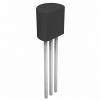
FQN1N60CTA Fairchild Semiconductor, FQN1N60CTA Datasheet - Page 2

FQN1N60CTA
Manufacturer Part Number
FQN1N60CTA
Description
MOSFET N-CH 600V 300MA TO-92
Manufacturer
Fairchild Semiconductor
Series
QFET™r
Datasheet
1.FQN1N60CTA.pdf
(8 pages)
Specifications of FQN1N60CTA
Fet Type
MOSFET N-Channel, Metal Oxide
Fet Feature
Standard
Rds On (max) @ Id, Vgs
11.5 Ohm @ 150mA, 10V
Drain To Source Voltage (vdss)
600V
Current - Continuous Drain (id) @ 25° C
300mA
Vgs(th) (max) @ Id
4V @ 250µA
Gate Charge (qg) @ Vgs
6.2nC @ 10V
Input Capacitance (ciss) @ Vds
170pF @ 25V
Power - Max
1W
Mounting Type
Through Hole
Package / Case
TO-92-3 (Standard Body), TO-226
Configuration
Single
Transistor Polarity
N-Channel
Resistance Drain-source Rds (on)
11.5 Ohm @ 10 V
Forward Transconductance Gfs (max / Min)
0.75 S
Drain-source Breakdown Voltage
600 V
Gate-source Breakdown Voltage
+/- 30 V
Continuous Drain Current
0.3 A
Power Dissipation
1000 mW
Maximum Operating Temperature
+ 150 C
Mounting Style
Through Hole
Minimum Operating Temperature
- 55 C
Lead Free Status / RoHS Status
Lead free / RoHS Compliant
Other names
FQN1N60CTA
FQN1N60CTATB
FQN1N60CTATB
Available stocks
Company
Part Number
Manufacturer
Quantity
Price
Company:
Part Number:
FQN1N60CTA
Manufacturer:
FSC
Quantity:
50 000
Part Number:
FQN1N60CTA
Manufacturer:
FAIRCHILD/仙童
Quantity:
20 000
FQN1N60C Rev. A
Package Marking and Ordering Information
Electrical Characteristics
Notes:
1. Repetitive Rating : Pulse width limited by maximum junction temperature
2. L = 59mH, I
3. I
4. Pulse Test : Pulse width
5. Essentially independent of operating temperature
6. a) Reference point of the R
Off Characteristics
BV
I
I
I
On Characteristics
V
R
g
Dynamic Characteristics
C
C
C
Switching Characteristics
t
t
t
t
Q
Q
Q
Drain-Source Diode Characteristics and Maximum Ratings
I
I
V
t
Q
d(on)
d(off)
DSS
GSSF
GSSR
r
f
S
SM
rr
b) When mounted on 3”x4.5” FR-4 PCB without any pad copper in a still air environment
FS
BV
T
GS(th)
DS(on)
iss
oss
rss
SD
SD
g
gs
gd
rr
Device Marking
J
DSS
Symbol
(R
DSS
0.3A, di/dt
JA
1N60C
/
is the sum of the junction-to-case and case-to-ambient thermal resistance. R
AS
= 1.1A, V
200A/ s, V
Drain-Source Breakdown Voltage
Breakdown Voltage Temperature
Coefficient
Zero Gate Voltage Drain Current
Gate-Body Leakage Current, Forward
Gate-Body Leakage Current, Reverse
Gate Threshold Voltage
Static Drain-Source
On-Resistance
Forward Transconductance
Input Capacitance
Output Capacitance
Reverse Transfer Capacitance
Turn-On Delay Time
Turn-On Rise Time
Turn-Off Delay Time
Turn-Off Fall Time
Total Gate Charge
Gate-Source Charge
Gate-Drain Charge
Maximum Continuous Drain-Source Diode Forward Current
Maximum Pulsed Drain-Source Diode Forward Current
Drain-Source Diode Forward Voltage
Reverse Recovery Time
Reverse Recovery Charge
DD
300 s, Duty cycle
= 50V, R
JL
DD
is the drain lead
FQN1N60C
BV
G
Device
DSS,
Parameter
= 25
Starting T
Starting T
2%
J
T
= 25°C
C
J
= 25°C unless otherwise noted
= 25°C
Package
TO-92
V
I
V
V
V
V
V
V
V
V
f = 1.0 MHz
V
R
V
V
V
V
dI
D
GS
DS
DS
GS
GS
DS
GS
DS
DS
DD
DS
GS
GS
GS
G
F
= 250 A, Referenced to 25°C
= 25
/ dt = 100 A/ s
= 0 V, I
= 600 V, V
= 480 V, T
= 30 V, V
= -30 V, V
= V
= 10 V, I
= 40 V, I
= 25 V, V
= 300 V, I
= 480 V, I
= 10 V
= 0 V, I
= 0 V, I
GS
2
Test Conditions
, I
CA
D
S
S
D
D
D
= 250 A
= 0.3 A
= 1.1 A,
GS
is determined by the user’s board design)
DS
D
D
= 250 A
DS
= 0.3 A
GS
C
= 0.15 A
= 1.1 A,
= 1.1 A,
Reel Size
= 125°C
= 0 V
= 0 V,
= 0 V
= 0 V
--
(Note 4, 5)
(Note 4, 5)
(Note 4)
(Note 4)
Tape Width
Min.
600
2.0
--
--
--
--
--
--
--
--
--
--
--
--
--
--
--
--
--
--
--
--
--
--
--
Typ.
0.75
0.53
130
190
0.6
9.3
3.5
4.8
0.7
2.7
19
21
13
27
--
--
--
--
--
--
--
--
--
7
Max.
-100
11.5
250
100
170
4.0
6.2
0.3
1.2
1.4
50
25
24
52
36
64
--
--
--
--
--
--
--
6
Quantity
www.fairchildsemi.com
2000ea
Units
V/°C
nA
nA
pF
pF
pF
nC
nC
nC
ns
ns
ns
ns
ns
V
V
S
A
A
V
C
A
A


