FQN1N60CTA Fairchild Semiconductor, FQN1N60CTA Datasheet

MOSFET N-CH 600V 300MA TO-92

FQN1N60CTA

Manufacturer Part Number
FQN1N60CTA
Description
MOSFET N-CH 600V 300MA TO-92
Manufacturer
Fairchild Semiconductor
Series
QFET™r
Datasheet

Specifications of FQN1N60CTA

Fet Type
MOSFET N-Channel, Metal Oxide
Fet Feature
Standard
Rds On (max) @ Id, Vgs
11.5 Ohm @ 150mA, 10V
Drain To Source Voltage (vdss)
600V
Current - Continuous Drain (id) @ 25° C
300mA
Vgs(th) (max) @ Id
4V @ 250µA
Gate Charge (qg) @ Vgs
6.2nC @ 10V
Input Capacitance (ciss) @ Vds
170pF @ 25V
Power - Max
1W
Mounting Type
Through Hole
Package / Case
TO-92-3 (Standard Body), TO-226
Configuration
Single
Transistor Polarity
N-Channel
Resistance Drain-source Rds (on)
11.5 Ohm @ 10 V
Forward Transconductance Gfs (max / Min)
0.75 S
Drain-source Breakdown Voltage
600 V
Gate-source Breakdown Voltage
+/- 30 V
Continuous Drain Current
0.3 A
Power Dissipation
1000 mW
Maximum Operating Temperature
+ 150 C
Mounting Style
Through Hole
Minimum Operating Temperature
- 55 C
Lead Free Status / RoHS Status
Lead free / RoHS Compliant
Other names
FQN1N60CTA
FQN1N60CTATB

Available stocks

Company
Part Number
Manufacturer
Quantity
Price
Part Number:
FQN1N60CTA
Manufacturer:
FSC
Quantity:
50 000
Part Number:
FQN1N60CTA
Manufacturer:
FAIRCHILD/仙童
Quantity:
20 000
Company:
Part Number:
FQN1N60CTA
Quantity:
990
Company:
Part Number:
FQN1N60CTA-G
Quantity:
22 000
Part Number:
FQN1N60CTA_G
Quantity:
2 628
©2005 Fairchild Semiconductor Corporation
FQN1N60C Rev. A
FQN1N60C
600V N-Channel MOSFET
Features
• 0.3 A, 600 V, R
• Low gate charge ( typical 4.8 nC )
• Low Crss ( typical 3.5 pF)
• Fast switching
• 100 % avalanche tested
• Improved dv/dt capability
Absolute Maximum Ratings
Thermal Characteristics
V
I
I
V
E
I
E
dv/dt
P
T
T
R
R
D
DM
AR
Symbol
Symbol
J
L
DSS
GSS
AS
AR
D
, T
JL
JA
STG
Drain-Source Voltage
Drain Current
Drain Current
Gate-Source Voltage
Single Pulsed Avalanche Energy
Avalanche Current
Repetitive Avalanche Energy
Peak Diode Recovery dv/dt
Power Dissipation (T
Operating and Storage Temperature Range
Maximum lead temperature for soldering purposes,
1/8" from case for 5 seconds
Thermal Resistance, Junction-to-Lead
Thermal Resistance, Junction-to-Ambient
DS(on)
= 11.5
G
D
S
- Continuous (T
- Continuous (T
- Pulsed
- Derate above 25°C
@ V
A
L
Parameter
Parameter
= 25°C)
= 25°C)
GS
= 10 V
C
C
TO-92
SSN Series
= 25°C)
= 100°C)
(Note 1)
(Note 2)
(Note 1)
(Note 1)
(Note 3)
(Note 6a)
(Note 6b)
1
Description
These N-Channel enhancement mode power field effect
transistors are produced using Fairchild’s proprietary, planar
stripe, DMOS technology.
This advanced technology has been especially tailored to
minimize on-state resistance, provide superior switching
performance, and withstand high energy pulse in the avalanche
and commutation mode. These devices are well suited for high
efficiency switched mode power supplies, active power factor
correction, electronic lamp ballasts based on half bridge
topology.
G
Typ
! ! ! !
! ! ! !
--
--
FQN1N60C
-55 to +150
◀ ◀ ◀ ◀
◀ ◀ ◀ ◀
D
! ! ! !
! ! ! !
! ! ! !
! ! ! !
S
0.18
0.02
● ●
● ●
● ●
● ●
● ●
● ●
600
300
0.3
1.2
0.3
0.3
4.5
33
1
3
30
▲ ▲ ▲ ▲
▲ ▲ ▲ ▲
Max
140
50
QFET
www.fairchildsemi.com
Units
Units
W/°C
V/ns
°C/W
°C/W
mJ
mJ
°C
°C
W
W
V
A
A
A
V
A
®

Related parts for FQN1N60CTA

FQN1N60CTA Summary of contents

Page 1

... Thermal Characteristics Symbol R Thermal Resistance, Junction-to-Lead JL R Thermal Resistance, Junction-to-Ambient JA ©2005 Fairchild Semiconductor Corporation FQN1N60C Rev. A Description = 10 V These N-Channel enhancement mode power field effect GS transistors are produced using Fairchild’s proprietary, planar stripe, DMOS technology. This advanced technology has been especially tailored to ...

Page 2

Package Marking and Ordering Information Device Marking Device 1N60C FQN1N60C Electrical Characteristics Symbol Parameter Off Characteristics BV Drain-Source Breakdown Voltage DSS BV / Breakdown Voltage Temperature DSS T Coefficient J I Zero Gate Voltage Drain Current DSS I Gate-Body Leakage ...

Page 3

Typical Performance Characteristics Figure 1. On-Region Characteristics V GS Top : 15.0 V 10.0 V 8 6.5 V 6.0 V 5.5 V 5.0 V Bottom : 4 ...

Page 4

Typical Performance Characteristics Figure 7. Breakdown Voltage Variation vs. Temperature 1.2 1.1 1.0 0.9 0.8 -100 - Junction Temperature [ J Figure 9. Maximum Safe Operating Area Operation in This Area is Limited by R DS(on) ...

Page 5

3mA 3mA 10V 10V Unclamped Inductive Switching Test Circuit & Waveforms 10V 10V FQN1N60C ...

Page 6

Driver ) ( Driver ) DUT ) ( DUT ) DUT ) ( DUT ) FQN1N60C Rev. A Peak Diode Recovery ...

Page 7

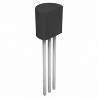
Mechanical Dimensions 0.46 1.27TYP [1.27 0.20 FQN1N60C Rev. A TO-92 +0.25 4.58 –0.15 0.10 1.27TYP ] [1.27 ] 0.20 3.60 0.20 (R2.29) 7 +0.10 0.38 –0.05 Dimensions in Millimeters www.fairchildsemi.com ...

Page 8

... TRADEMARKS The following are registered and unregistered trademarks Fairchild Semiconductor owns or is authorized to use and is not intended exhaustive list of all such trademarks. FAST ® ACEx™ ActiveArray™ FASTr™ Bottomless™ FPS™ Build it Now™ FRFET™ CoolFET™ ...

Related keywords