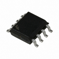
FDS6681Z Fairchild Semiconductor, FDS6681Z Datasheet - Page 3

FDS6681Z
Manufacturer Part Number
FDS6681Z
Description
MOSFET P-CH 30V 20A SO-8
Manufacturer
Fairchild Semiconductor
Series
PowerTrench®r
Datasheet
1.FDS6681Z.pdf
(6 pages)
Specifications of FDS6681Z
Fet Type
MOSFET P-Channel, Metal Oxide
Fet Feature
Logic Level Gate
Rds On (max) @ Id, Vgs
4.6 mOhm @ 20A, 10V
Drain To Source Voltage (vdss)
30V
Current - Continuous Drain (id) @ 25° C
20A
Vgs(th) (max) @ Id
3V @ 250µA
Gate Charge (qg) @ Vgs
260nC @ 10V
Input Capacitance (ciss) @ Vds
7540pF @ 15V
Power - Max
1W
Mounting Type
Surface Mount
Package / Case
8-SOIC (3.9mm Width)
Configuration
Single Quad Drain Triple Source
Transistor Polarity
P-Channel
Resistance Drain-source Rds (on)
0.0046 Ohm @ 10 V
Forward Transconductance Gfs (max / Min)
79 S
Drain-source Breakdown Voltage
30 V
Gate-source Breakdown Voltage
+/- 25 V
Continuous Drain Current
20 A
Power Dissipation
2500 mW
Maximum Operating Temperature
+ 150 C
Mounting Style
SMD/SMT
Minimum Operating Temperature
- 55 C
Lead Free Status / RoHS Status
Lead free / RoHS Compliant
Other names
FDS6681Z
FDS6681ZTR
FDS6681ZTR
Available stocks
Company
Part Number
Manufacturer
Quantity
Price
Company:
Part Number:
FDS6681Z
Manufacturer:
Fairchild Semiconductor
Quantity:
375 013
Part Number:
FDS6681Z
Manufacturer:
FAIRCHILD/仙童
Quantity:
20 000
I
V
Drain–Source Diode Characteristics and Maximum Ratings
t
Electrical Characteristics
Symbol
Q
Notes:
1. R
Scale 1 : 1 on letter size paper
2. Pulse Test: Pulse Width < 300µs, Duty Cycle < 2.0%
3. The diode connected between the gate and source serves only as protection against ESD. No gate overvoltage rating is implied.
S
RR
SD
RR
drain pins. R
θJA
is the sum of the junction-to-case and case-to-ambient thermal resistance where the case thermal reference is defined as the solder mounting surface of the
θJC
Maximum Continuous Drain–Source Diode Forward Current
Drain–Source Diode Forward
Voltage
Reverse Recovery Time
Reverse Recovery Charge
is guaranteed by design while R
a) 50°C/W (10 sec)
62.5°C/W steady state
when mounted on a
1in
copper
Parameter
2
pad of 2 oz
θCA
is determined by the user's board design.
T
A
V
I
dI
= 25°C unless otherwise noted
F
GS
F
= –20 A,
/dt = 100 A/µs
= 0 V,
b) 105°C/W when
Test Conditions
mounted on a .04 in
pad of 2 oz copper
I
S
= –2.1 A
2
(Note 2)
(Note 2)
Min
c) 125°C/W when mounted
Typ
on a minimum pad.
–0.7
125
94
Max Units
–2.1
–1.2
FDS6681Z Rev B (W)
nC
ns
A
V


