HUFA76504DK8T Fairchild Semiconductor, HUFA76504DK8T Datasheet
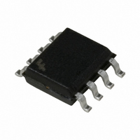
MOSFET N-CHAN 80V 2.3A 8-SOIC

HUFA76504DK8T

Manufacturer Part Number
HUFA76504DK8T
Description
MOSFET N-CHAN 80V 2.3A 8-SOIC
Manufacturer
Fairchild Semiconductor
Series
UltraFET™r
Datasheet

Specifications of HUFA76504DK8T

Fet Type
2 N-Channel (Dual)
Fet Feature
Logic Level Gate
Rds On (max) @ Id, Vgs
200 mOhm @ 2.5A, 10V
Drain To Source Voltage (vdss)
80V
Current - Continuous Drain (id) @ 25° C
2.3A
Vgs(th) (max) @ Id
3V @ 250µA
Gate Charge (qg) @ Vgs
10nC @ 10V
Input Capacitance (ciss) @ Vds
270pF @ 25V
Power - Max
2.5W
Mounting Type
Surface Mount
Package / Case
8-SOIC (3.9mm Width)
Configuration
Dual Dual Drain
Transistor Polarity
N-Channel
Resistance Drain-source Rds (on)
0.173 Ohms
Forward Transconductance Gfs (max / Min)
0.00008 S
Drain-source Breakdown Voltage
80 V
Gate-source Breakdown Voltage
+/- 16 V
Continuous Drain Current
2.3 A
Power Dissipation
2.5 W
Maximum Operating Temperature
+ 150 C
Mounting Style
SMD/SMT
Minimum Operating Temperature
- 55 C
Lead Free Status / RoHS Status
Lead free / RoHS Compliant
2.3A, 80V, 0.222 Ohm, Dual N-Channel,
Logic Level UltraFET Power MOSFET
Packaging
Symbol
Absolute Maximum Ratings
Drain to Source Voltage (Note 1). . . . . . . . . . . . . . . . . . . . . . . . . . . . . . . . . . . . . . . . . . V
Drain to Gate Voltage (R
Gate to Source Voltage . . . . . . . . . . . . . . . . . . . . . . . . . . . . . . . . . . . . . . . . . . . . . . . . . . V
Drain Current
Pulsed Avalanche Rating . . . . . . . . . . . . . . . . . . . . . . . . . . . . . . . . . . . . . . . . . . . . . . . . .UIS
Power Dissipation (Note 2) . . . . . . . . . . . . . . . . . . . . . . . . . . . . . . . . . . . . . . . . . . . . . . . . P
Operating and Storage Temperature . . . . . . . . . . . . . . . . . . . . . . . . . . . . . . . . . . . . T
Maximum Temperature for Soldering
NOTES:
CAUTION: Stresses above those listed in “Absolute Maximum Ratings” may cause permanent damage to the device. This is a stress only rating and operation of the
device at these or any other conditions above those indicated in the operational sections of this specification is not implied.
This product has been designed to meet the extreme test conditions and environment demanded by the automotive industry. For a copy
All Fairchild semiconductor products are manufactured, assembled and tested under ISO9000 and QS9000 quality systems certification.
©2001 Fairchild Semiconductor Corporation
1. T
2. 50
3. 228
Continuous (T
Continuous (T
Continuous (T
Continuous (T
Pulsed Drain Current . . . . . . . . . . . . . . . . . . . . . . . . . . . . . . . . . . . . . . . . . . . . . . . . . . .I
Derate Above 25
Leads at 0.063in (1.6mm) from Case for 10s. . . . . . . . . . . . . . . . . . . . . . . . . . . . . . . . . .T
Package Body for 10s, See Techbrief TB334 . . . . . . . . . . . . . . . . . . . . . . . . . . . . . . . T
J
o
= 25
C/W measured using FR-4 board with 0.76 in
o
SOURCE1 (1)
SOURCE2 (3)
C/W measured using FR-4 board with 0.006 in
o
GATE1 (2)
GATE2 (4)
C to 125
A
A
A
A
= 25
= 25
= 100
= 100
1
o
BRANDING DASH
C . . . . . . . . . . . . . . . . . . . . . . . . . . . . . . . . . . . . . . . . . . . . . . . . . . . . . . .
o
2
o
o
C.
C, V
C, V
o
o
JEDEC MS-012AA
GS
C, V
C, V
3
GS
GS
= 20k ) (Note 1) . . . . . . . . . . . . . . . . . . . . . . . . . . . . . . . . V
4
GS
GS
= 5V) (Note 2) . . . . . . . . . . . . . . . . . . . . . . . . . . . . . . . . . . I
= 10V) (Figure 2) (Note 2) . . . . . . . . . . . . . . . . . . . . . . . . . I
Reliability data can be found at: http://www.mtp.intersil.com/automotive.html.
= 5V) (Note 3) . . . . . . . . . . . . . . . . . . . . . . . . . . . . . . . . . I
= 4.5V) (Figure 2) (Note 3). . . . . . . . . . . . . . . . . . . . . . . . I
of the requirements, see AEC Q101 at: http://www.aecouncil.com/
T
Data Sheet
A
= 25
o
DRAIN 1 (8)
DRAIN 1 (7)
DRAIN 2 (6)
DRAIN 2 (5)
5
C, Unless Otherwise Specified
UltraFET® is a registered trademark of Fairchild Corporation. PSPICE® is a registered trademark of Cadence Corporation.
2
(490.3 mm
2
(3.87 mm
CAUTION: These devices are sensitive to electrostatic discharge; follow proper ESD Handling Procedures.
2
) copper pad at 1 second.
2
) copper pad at 1000 seconds.
Features
• Ultra Low On-Resistance
• Simulation Models
• Internal R
• Peak Current vs Pulse Width Curve
• UIS Rating Curve
• Transient Thermal Impedance Curve vs Board Mounting
Ordering Information
NOTE: When ordering, use the entire part number. Add the suffix T
to obtain the variant in tape and reel, e.g., HUFA76504DK8T.
HUFA76504DK8
- r
- r
- Temperature Compensated PSPICE™ and SABER
- Spice and SABER Thermal Impedance Models
- www.Fairchildsemi.com
Area
PART NUMBER
Electrical Models
J
DS(ON)
DS(ON)
, T
DGR
DSS
STG
DM
pkg
GS
D
D
D
D
D
L
G
= 0.200
= 0.222
June 2001
= 50
SABER© is a
MS-012AA
V
V
PACKAGE
GS
GS
HUFA76504DK8
Figures 6, 17, 18
HUFA76504DK8
registered trademark
-55 to 150
Figure 4
10V
5V
300
260
2.3
2.5
1.1
1.1
2.5
80
80
20
16
76504DK8
of Avanti corporation.
BRAND
Rev. A, June 4, 2001
mW/
UNITS
o
o
o
W
V
V
V
A
A
A
A
C
C
C
o
C

Related parts for HUFA76504DK8T

HUFA76504DK8T Summary of contents

Page 1

... DRAIN 1 (8) Area DRAIN 1 (7) Ordering Information DRAIN 2 (6) PART NUMBER DRAIN 2 (5) HUFA76504DK8 NOTE: When ordering, use the entire part number. Add the suffix T to obtain the variant in tape and reel, e.g., HUFA76504DK8T Unless Otherwise Specified , (490 copper pad at 1 second. ...

Page 2

... Gate to Drain “Miller” Charge CAPACITANCE SPECIFICATIONS Input Capacitance Output Capacitance Reverse Transfer Capacitance Source to Drain Diode Specifications PARAMETER Source to Drain Diode Voltage Reverse Recovery Time Reverse Recovered Charge ©2001 Fairchild Semiconductor Corporation o C, Unless Otherwise Specified SYMBOL TEST CONDITIONS 250 (Figure 12) DSS ...

Page 3

... FIGURE 3. NORMALIZED MAXIMUM TRANSIENT THERMAL IMPEDANCE 200 TRANSCONDUCTANCE MAY LIMIT CURRENT 100 IN THIS REGION V = 10V 4. ©2001 Fairchild Semiconductor Corporation 100 125 150 o C) FIGURE 2. MAXIMUM CONTINUOUS DRAIN CURRENT vs SINGLE PULSE - RECTANGULAR PULSE DURATION ( PULSE WIDTH (s) FIGURE 4. PEAK CURRENT CAPABILITY 3.0 2 ...

Page 4

... I = 1.1A D 200 150 GATE TO SOURCE VOLTAGE (V) GS FIGURE 9. DRAIN TO SOURCE ON RESISTANCE vs GATE VOLTAGE AND DRAIN CURRENT ©2001 Fairchild Semiconductor Corporation (Continued) 100 s 1ms 10ms 100 200 NOTE: Refer to Application Notes AN9321 and AN9322. FIGURE 6. UNCLAMPED INDUCTIVE SWITCHING 3.5 4.0 4.5 PULSE DURATION = 80 s DUTY CYCLE = 0 ...

Page 5

... V , DRAIN TO SOURCE VOLTAGE (V) DS FIGURE 13. CAPACITANCE vs DRAIN TO SOURCE VOLTAGE 4.5V 40V 1. GATE TO SOURCE RESISTANCE ( ) GS FIGURE 15. SWITCHING TIME vs GATE RESISTANCE ©2001 Fairchild Semiconductor Corporation (Continued 250 120 160 o C) FIGURE 12. NORMALIZED DRAIN TO SOURCE BREAKDOWN ISS NOTE: Refer to Application Notes AN7254 and AN7260. ...

Page 6

... Test Circuits and Waveforms VARY t TO OBTAIN P R REQUIRED PEAK FIGURE 17. UNCLAMPED ENERGY TEST CIRCUIT g(REF) FIGURE 19. GATE CHARGE TEST CIRCUIT FIGURE 21. SWITCHING TIME TEST CIRCUIT ©2001 Fairchild Semiconductor Corporation DUT 0. DUT g(REF DUT DSS FIGURE 18. UNCLAMPED ENERGY WAVEFORMS Q g(TOT) ...

Page 7

... JA times a cofficient added to a constant. The area, in square inches is the top copper area including the gate and source pads. = – 103.2 24.3 Area JA ©2001 Fairchild Semiconductor Corporation , and the C/ never exceeded. (EQ. 1) FIGURE 23. THERMAL RESISTANCE vs MOUNTING PAD AREA ...

Page 8

... FIGURE 24. THERMAL RESISTANCE vs MOUNTING PAD AREA ©2001 Fairchild Semiconductor Corporation ) is also effected by Copper pad area has no perceivable effect on transient JA thermal impedance for pulse widths less than 100ms. For pulse widths less than 100ms the transient thermal impedance is determined by the die and package. Therefore, CTHERM1 through CTHERM5 and RTHERM1 through RTHERM5 remain constant for each of the thermal models ...

Page 9

... NOTE: For further discussion of the PSPICE model, consult A New PSPICE Sub-Circuit for the Power MOSFET Featuring Global Temperature Options; IEEE Power Electronics Specialist Conference Records, 1991, written by William J. Hepp and C. Frank Wheatley. ©2001 Fairchild Semiconductor Corporation REV 18 January 2001 DPLCAP ...

Page 10

... Fairchild Semiconductor Corporation DPLCAP 10 RSLC2 - 6 ESG 8 EVTHRES + ...

Page 11

... COMPONANT 0.02 in CTHERM6 9.0e-2 CTHERM7 4.0e-1 CTHERM8 1.4 RTHERM6 RTHERM7 RTHERM8 ©2001 Fairchild Semiconductor Corporation RTHERM1 RTHERM2 RTHERM3 RTHERM4 RTHERM5 RTHERM6 RTHERM7 RTHERM8 TABLE 1. Thermal Models 2 2 0.14 in 1.3e-1 6.0e-1 2 ...

Page 12

... MS-012AA 8 LEAD JEDEC MS-012AA SMALL OUTLINE PLASTIC PACKAGE 0.060 1.52 0.155 4.0 0.275 7.0 MINIMUM RECOMMENDED FOOTPRINT FOR SURFACE-MOUNTED APPLICATIONS MS-012AA 12mm TAPE AND REEL ©2001 Fairchild Semiconductor Corporation SYMBOL NOTES: 1. All dimensions are within allowable dimensions of Rev JEDEC MS-012AA outline dated 5-90. ...

Page 13

... TRADEMARKS The following are registered and unregistered trademarks Fairchild Semiconductor owns or is authorized to use and is not intended exhaustive list of all such trademarks. ACEx™ FAST Bottomless™ FASTr™ CoolFET™ FRFET™ CROSSVOLT™ GlobalOptoisolator™ GTO™ DenseTrench™ ...

Related keywords