FDG6318PZ Fairchild Semiconductor, FDG6318PZ Datasheet
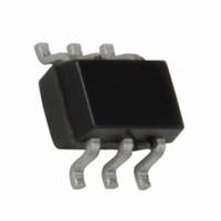
MOSFET P-CH DUAL 20V SC70-6

FDG6318PZ

Manufacturer Part Number
FDG6318PZ
Description
MOSFET P-CH DUAL 20V SC70-6
Manufacturer
Fairchild Semiconductor
Datasheets

Specifications of FDG6318PZ

Fet Type
2 P-Channel (Dual)
Fet Feature
Logic Level Gate
Rds On (max) @ Id, Vgs
780 mOhm @ 500mA, 4.5V
Drain To Source Voltage (vdss)
20V
Current - Continuous Drain (id) @ 25° C
500mA
Vgs(th) (max) @ Id
1.5V @ 250µA
Gate Charge (qg) @ Vgs
1.62nC @ 4.5V
Input Capacitance (ciss) @ Vds
85.4pF @ 10V
Power - Max
300mW
Mounting Type
Surface Mount
Package / Case
SC-70-6, SC-88, SOT-363
Configuration
Dual
Transistor Polarity
P-Channel
Resistance Drain-source Rds (on)
0.78 Ohm @ 4.5 V
Forward Transconductance Gfs (max / Min)
1.1 S
Drain-source Breakdown Voltage
20 V
Gate-source Breakdown Voltage
+/- 12 V
Continuous Drain Current
0.5 A
Power Dissipation
300 mW
Maximum Operating Temperature
+ 150 C
Mounting Style
SMD/SMT
Minimum Operating Temperature
- 55 C
Lead Free Status / RoHS Status
Lead free / RoHS Compliant

Available stocks

Company
Part Number
Manufacturer
Quantity
Price
Part Number:
FDG6318PZ
Manufacturer:
FAIRCHILD
Quantity:
30 000
FDG6318P
Dual P-Channel, Digital FET
General Description
These dual P-Channel logic level enhancement mode
MOSFET are produced using Fairchild Semiconductor’s
advanced
especially tailored to minimize on-state resistance. This
device has been designed especially for low voltage
applications as a replacement for bipolar digital
transistors and small signal MOSFETS.
Applications
2003 Fairchild Semiconductor Corporation
Absolute Maximum Ratings
Symbol
V
V
I
P
T
Thermal Characteristics
R
Package Marking and Ordering Information
D
Battery management
J
DSS
GSS
D
, T
JA
Device Marking
STG
.38
PowerTrench
Drain-Source Voltage
Gate-Source Voltage
Drain Current
Power Dissipation for Single Operation
Operating and Storage Junction Temperature Range
Thermal Resistance, Junction-to-Ambient
D
Pin 1
G
S
process
SC70-6
– Continuous
– Pulsed
The pinouts are symmetrical; pin 1 and pin 4 are interchangeable.
FDG6318P
S
Device
Parameter
G
that
D
has
T
A
been
=25
o
C unless otherwise noted
Reel Size
7’’
(Note 1)
(Note 1)
(Note 1)
Features
–0.5 A, –20 V.
Very low level gate drive requirements allowing direct
operation in 3V circuits (V
Compact industry standard SC70-6 surface mount
package
G
S
D
1 or 4
2 or 5
3 or 6
Tape width
–55 to +150
8mm
R
R
Ratings
DS(ON)
DS(ON)
–0.5
–1.8
–20
±12
415
0.3
= 780 m @ V
= 1200 m @ V
GS(th)
< 1.5V).
4 or 1
6 or 3
5 or 2
January 2003
G
D
S
FDG6318P Rev C (W)
GS
3000 units
Quantity
GS
= –4.5 V
= –2.5 V
Units
C/W
W
V
V
A
C

Related parts for FDG6318PZ

FDG6318PZ Summary of contents

Page 1

... FDG6318P Dual P-Channel, Digital FET General Description These dual P-Channel logic level enhancement mode MOSFET are produced using Fairchild Semiconductor’s advanced PowerTrench process especially tailored to minimize on-state resistance. This device has been designed especially for low voltage applications as a replacement for bipolar digital transistors and small signal MOSFETS ...

Page 2

Electrical Characteristics Symbol Parameter Off Characteristics BV Drain–Source Breakdown DSS Voltage Breakdown Voltage Temperature BV DSS Coefficient Zero Gate Voltage Drain Current DSS I Gate–Body Leakage GSS On Characteristics (Note 2) V Gate Threshold Voltage GS(th) Gate ...

Page 3

Typical Characteristics 1.8 -3. -10.0V GS -4.5V -6.0V 1.2 0 0 DRAIN-SOURCE VOLTAGE (V) DS Figure 1. On-Region Characteristics. 1 -0. -4.5V GS 1.2 1.1 1 ...

Page 4

Typical Characteristics -0. - -15V 0.3 0.6 0.9 1 GATE CHARGE (nC) g Figure 7. Gate Charge Characteristics LIMIT DS(ON) 1 10ms 100ms ...

Page 5

CROSSVOLT â â â â â Rev. I2 ...

Related keywords