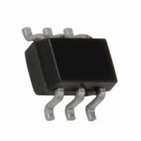
FDG6318PZ Fairchild Semiconductor, FDG6318PZ Datasheet

FDG6318PZ
Specifications of FDG6318PZ
Available stocks
Related parts for FDG6318PZ
FDG6318PZ Summary of contents
Page 1
... A Parameter 4.5V 2.5V) GS Package Reel Size SC70-6 January 2003 r = 780m Max)@ V DS(ON 1200m Max DS(ON) GS < 1.5V). GS(TH Ratings -20 12 -0.5 -0.3 Figure 4 0.3 2.4 -55 to 150 1.4 415 Tape Width Quantity 7” 3000 FDG6318PZ Rev -4 -2.5 V Units mW C/W ...
Page 2
... -0.5A, dI /dt = 100A determined by user’s board design Min Typ Max - -0.65 -0.9 -1.5 - 580 780 - 910 1200 - 1.08 1.62 = -10V DD - 0.67 1.0 = -0. 0. 1.0mA -0.9 -1 415 C/W when mounted on a 1inch JA FDG6318PZ Rev. B Units copper pad. ...
Page 3
... Figure 2. Maximum Continuous Drain Current RECTANGULAR PULSE DURATION (s) = -2. PULSE WIDTH (s) Figure 4. Peak Current Capability V = -4. -2. 100 125 CASE TEMPERATURE ( C) A Case Temperature NOTES: DUTY FACTOR t1/t2 PEAK FOR TEMPERATURES o ABOVE 25 C DERATE PEAK CURRENT AS FOLLOWS: 150 - 125 FDG6318PZ Rev. B 150 ...
Page 4
... GS D 0.6 80 120 160 - Figure 10. Normalized Gate Threshold Voltage vs = -10V 150 - GATE TO SOURCE VOLTAGE (V) GS PULSE DURATION = 80 s DUTY CYCLE = 0.5% MAX I = -0. -0. GATE TO SOURCE VOLTAGE (V) GS Voltage and Drain Current 250 - 120 JUNCTION TEMPERATURE ( C) J Junction Temperature FDG6318PZ Rev 160 ...
Page 5
... Figure 13. Gate Charge Waveforms for Constant Gate Currents ©2003 Fairchild Semiconductor Corporation (Continued 25°C unless otherwise noted A 200 100 120 160 0 Figure 12. Capacitance vs Drain to Source -10V WAVEFORMS IN 2 DESCENDING ORDER -0. -0. 0.5 1.0 Qg, GATE CHARGE (nC ISS OSS RSS 0V 1MHz DRAIN TO SOURCE VOLTAGE (V) DS Voltage 1.5 2.0 FDG6318PZ Rev ...
Page 6
... PSPICE Electrical Model .SUBCKT FDG6318PZ rev January 2003 0.6e- 1.1e-10 CIN 6 8 0.75e-10 DBODY 5 7 DBODYMOD DBREAK 7 11 DBREAKMOD DPLCAP 10 6 DPLCAPMOD EBREAK -23.3 EDS EGS ESG EVTHRES EVTEMP LGATE GATE LDRAIN 2 5 1e-9 1 LGATE 1 9 0.47e-9 RLGATE LSOURCE 3 7 0.47e-9 ...
Page 7
... DPLCAP EVTHRES + 19 EVTEMP LGATE 8 RGATE + RLGATE CIN S1A S2A S1B S2B EDS EGS 8 8 LDRAIN RLDRAIN RSLC1 ISCL EBREAK 18 50 RDRAIN DBODY MWEAK MMED DBREAK MSTRO LSOURCE RSOURCE 8 7 RLSOURCE RBREAK 18 17 RVTEMP 19 IT VBAT + 8 22 RVTHRES FDG6318PZ Rev. B DRAIN 2 SOURCE 3 ...
Page 8
... CTHERM8 c8 Ambient 0.29 RTHERM1 Junction c2 11.2 RTHERM2 c2 c3 11.5 RTHERM3 c3 c4 12.5 RTHERM4 RTHERM5 RTHERM6 RTHERM7 RTHERM8 c8 Ambient 93 SABER Thermal Model SABER thermal model FDG6318PZ Copper Area= 1sq.in template thermal_model th tl thermal_c th ctherm.ctherm1 0.17e-4 ctherm.ctherm2 2.7e-4 ctherm.ctherm3 5.5e-4 ctherm.ctherm4 1.4e-3 ctherm.ctherm5 2.2e-3 ctherm ...
Page 9
... TRADEMARKS The following are registered and unregistered trademarks Fairchild Semiconductor owns or is authorized to use and is not intended exhaustive list of all such trademarks. ACEx™ FACT™ ActiveArray™ FACT Quiet Series™ ® Bottomless™ FAST CoolFET™ FASTr™ CROSSVOLT™ ...


