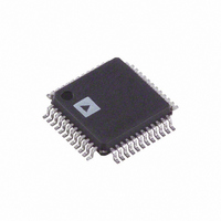
ADUC7032BSTZ-8L-RL Analog Devices Inc, ADUC7032BSTZ-8L-RL Datasheet - Page 93

ADUC7032BSTZ-8L-RL
Manufacturer Part Number
ADUC7032BSTZ-8L-RL
Description
IC,Battery Management,QFP,48PIN,PLASTIC
Manufacturer
Analog Devices Inc
Series
MicroConverter® ADuC7xxxr
Datasheet
1.EVAL-ADUC7032QSPZ.pdf
(116 pages)
Specifications of ADUC7032BSTZ-8L-RL
Core Processor
ARM7
Core Size
16/32-Bit
Speed
20.48MHz
Connectivity
LIN, SPI, UART/USART
Peripherals
POR, PSM, Temp Sensor, WDT
Number Of I /o
9
Program Memory Size
96KB (96K x 8)
Program Memory Type
FLASH
Ram Size
6K x 8
Voltage - Supply (vcc/vdd)
3.5 V ~ 18 V
Data Converters
A/D 2x16b
Oscillator Type
Internal
Operating Temperature
-40°C ~ 105°C
Package / Case
48-LQFP
Lead Free Status / RoHS Status
Lead free / RoHS Compliant
Eeprom Size
-
Lead Free Status / Rohs Status
Compliant
WU (WAKE-UP) PIN
The WU (wake-up) pin is a high voltage GPIO controlled via
HVCON and HVDAT.
WU Pin Circuit Description
The WU pin is configured by default as an output with an
internal 10 kΩ pull-down resistor and high-side FET driver.
The WU pin, in its default mode of operation, is specified to
generate an active high system wake-up request by forcing the
external system WU bus high. User code can assert the WU
output by writing directly to HVCFG0[4].
It should be noted that the output responds only after the 10 μs
latency through the (serial communication based) high voltage
interface.
The internal FET is capable of sourcing significant current and,
therefore, a substantial on-chip self-heating can occur if this
driver is asserted for a long time period. For this reason,
a monoflop (a 1.3-second timeout timer) has been included.
OUTPUT CONTROL
SHORT-CIRCUIT
PROTECTION
HVCFG0[4]
HVMON[0]
HVMON[7]
NORMAL
NORMAL
IMMUNITY
GLITCH
400µs
READBACK
HVCFG1[4]
ENABLE
SHORT-CIRCUIT
TRIP REFERENCE
3V
Figure 36. WU Circuit, Block Diagram
Rev.0 | Page 93 of 116
IO_VSS
VDD
INTERNAL
SENSE
RESISTOR
6kΩ
INTERNAL
10kΩ
RESISTOR
By default, the monoflop is enabled and disables the WU driver
after 1.3 seconds. It is possible to disable the monoflop via
HVCFG1[1]. If the WU monoflop is disabled, then the WU
driver should be disabled after 1.3 seconds.
The WU pin also features a short-circuit detection feature.
When the WU pin sources more than 200 mA for 400 μs,
a high voltage interrupt is generated with HVMON[0] set.
By default, a thermal shutdown event disables the WU driver.
The WU driver must be re-enabled manually after a thermal
event via HVCFG1[3]. It is possible to disable the automatic
shutdown during a thermal event via HVCFG0[7].
The WU pin can be configured in I/O mode by writing a 1 to
HVCFG1[4]. In this mode, a rising or falling edge immediately
generates a high voltage interrupt. HVMON[7] directly reflects
the state of the external WU pin. This comparator has a trip
level of 3 V typical.
OPEN-CIRCUIT
DIAGNOSTIC
RESISTOR
HVCFG1[0]
EXTERNAL
WU PIN
CURRENT-LIMIT
EXTERNAL
RESISTOR
39Ω
C
91nF
LOAD
R
1kΩ
ADuC7032-8L
LOAD
EXTERNAL
WAKE BUS


