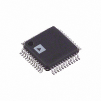
ADUC7032BSTZ-8L-RL Analog Devices Inc, ADUC7032BSTZ-8L-RL Datasheet - Page 79

ADUC7032BSTZ-8L-RL
Manufacturer Part Number
ADUC7032BSTZ-8L-RL
Description
IC,Battery Management,QFP,48PIN,PLASTIC
Manufacturer
Analog Devices Inc
Series
MicroConverter® ADuC7xxxr
Datasheet
1.EVAL-ADUC7032QSPZ.pdf
(116 pages)
Specifications of ADUC7032BSTZ-8L-RL
Core Processor
ARM7
Core Size
16/32-Bit
Speed
20.48MHz
Connectivity
LIN, SPI, UART/USART
Peripherals
POR, PSM, Temp Sensor, WDT
Number Of I /o
9
Program Memory Size
96KB (96K x 8)
Program Memory Type
FLASH
Ram Size
6K x 8
Voltage - Supply (vcc/vdd)
3.5 V ~ 18 V
Data Converters
A/D 2x16b
Oscillator Type
Internal
Operating Temperature
-40°C ~ 105°C
Package / Case
48-LQFP
Lead Free Status / RoHS Status
Lead free / RoHS Compliant
Eeprom Size
-
Lead Free Status / Rohs Status
Compliant
GPIO Port0 Control Register
Name: GP0CON
Address: 0xFFFF0D00
Default Value: 0x11100000
Access: Read/write
Function: This 32-bit MMR selects the pin function for each Port0 pin.
Table 59. GP0CON MMR Bit Designations
Bit
31 to 29
28
27 to 25
24
23 to 21
20
19 to 17
16
15 to 13
12
11 to 9
8
7 to 5
4
3 to 1
0
Description
Reserved. These bits are reserved and should be written as 0 by user code.
Reserved. This bit is reserved and should be written as 1 by user code.
Reserved. These bits are reserved and should be written as 0 by user code.
Internal P0.6 Enable Bit. This bit must be set to 1 by user software to enable the high voltage serial interface before using the
HVCON and HVDAT registered high voltage interface.
Reserved. These bits are reserved and should be written as 0 by user code.
Internal P0.5 Enable Bit. This bit must be set to 1 by user software to enable the high voltage serial interface before using the
HVCON and HVDAT registered high voltage interface.
Reserved. These bits are reserved and should be written as 0 by user code.
GPIO_4 Function Select Bit.
Reserved. These bits are reserved and should be written as 0 by user code.
GPIO_3 Function Select Bit.
Reserved. These bits are reserved and should be written as 0 by user code.
GPIO_2 Function Select Bit.
Reserved. These bits are reserved and should be written as 0 by user code.
GPIO_1 Function Select Bit.
Reserved. These bits are reserved and should be written as 0 by user code.
GPIO_0 Function Select Bit.
Cleared to 0 by user code to configure the GPIO_4 pin as a general-purpose I/O (GPIO) pin.
Set to 1 by user code to configure the GPIO_4 pin as ECLK, enabling a 2.56 MHz clock output on this pin.
Cleared to 0 by user code to configure the GPIO_3 pin as a general-purpose I/O (GPIO) pin.
Set to 1 by user code to configure the GPIO_2 pin as MOSI (master output, slave input) data for the SPI port.
Cleared to 0 by user code to configure the GPIO_2 pin as a general-purpose I/O (GPIO) pin.
Set to 1 by user code to configure the GPIO_3 pin as MISO (master input, slave output) data for the SPI port.
Cleared to 0 by user code to configure the GPIO_1 pin as a general-purpose I/O (GPIO) pin.
Set to 1 by user code to configure the GPIO_1 pin as SCLK, serial clock I/O for the SPI port.
Cleared to 0 by user code to configure the GPIO_0 pin as a general-purpose I/O (GPIO) pin.
Set to 1 by user code to configure the GPIO_0 pin as an SS (slave select) I/O for the SPI port.
Rev.0 | Page 79 of 116
ADuC7032-8L


