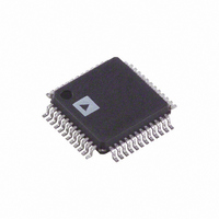
ADUC7032BSTZ-8L-RL Analog Devices Inc, ADUC7032BSTZ-8L-RL Datasheet - Page 68

ADUC7032BSTZ-8L-RL
Manufacturer Part Number
ADUC7032BSTZ-8L-RL
Description
IC,Battery Management,QFP,48PIN,PLASTIC
Manufacturer
Analog Devices Inc
Series
MicroConverter® ADuC7xxxr
Datasheet
1.EVAL-ADUC7032QSPZ.pdf
(116 pages)
Specifications of ADUC7032BSTZ-8L-RL
Core Processor
ARM7
Core Size
16/32-Bit
Speed
20.48MHz
Connectivity
LIN, SPI, UART/USART
Peripherals
POR, PSM, Temp Sensor, WDT
Number Of I /o
9
Program Memory Size
96KB (96K x 8)
Program Memory Type
FLASH
Ram Size
6K x 8
Voltage - Supply (vcc/vdd)
3.5 V ~ 18 V
Data Converters
A/D 2x16b
Oscillator Type
Internal
Operating Temperature
-40°C ~ 105°C
Package / Case
48-LQFP
Lead Free Status / RoHS Status
Lead free / RoHS Compliant
Eeprom Size
-
Lead Free Status / Rohs Status
Compliant
ADuC7032-8L
TIMERS
The ADuC7032-8L features four general-purpose
timers/counters.
•
•
•
•
The four timers in their normal mode of operation can be either
free-running or periodic.
In free-running mode, the counter decrements/increments
from the maximum/minimum value until zero/full scale and
starts again at the maximum/minimum value.
Table 53. Timer Event Capture
Bit
0
1
2
3
4
5
6
7
8
9
10
11
12
13
14
15
16
17
Timer0, or lifetime timer
Timer1
Timer2 or wake-up timer
Timer3 or watchdog timer
Description
Timer0.
Timer1.
Timer2 or Wake-Up Timer.
Timer3 or Watchdog Timer.
Reserved.
LIN Hardware.
Flash/EE Interrupt.
PLL Lock.
ADC.
UART.
SPI Master.
XIRQ0 (GPIO IRQ 0).
XIRQ1 (GPIO IRQ 1).
Reserved.
IRQ3 High Voltage IRQ.
SPI Slave.
XIRQ4 (GPIO IRQ 4).
XIRQ5 (GPIO IRQ 5).
Comments
See the Timer0—Lifetime Timer section.
See the Timer1 section.
See the Timer2—Wake-Up Timer section.
See the Timer3—Watchdog Timer section.
Should be written as 0.
See the LIN (Local Interconnect Network) Interface section.
See the Flash/EE Control Interface section.
See the ADUC7032-8L System Clocks section.
See the 16-Bit, Sigma-Delta Analog-to-Digital Converters section.
See the UART Serial Interface section.
See the Serial Peripheral Interface section.
See the General-Purpose I/O section.
See the General-Purpose I/O section.
Should be written as 0.
See the High Voltage Peripheral Control Interface section.
See the General-Purpose I/O section.
See the General-Purpose I/O section.
Rev.0 | Page 68 of 116
In periodic mode, the counter decrements/increments from the
value in the load register (TxLD MMR) until zero/full scale and
starts again at the value stored in the load register.
The value of a counter can be read at any time by accessing its
value register (TxVAL). Timers are started by writing in the
control register of the corresponding timer (TxCON).
In normal mode, an IRQ is generated each time the value of the
counter reaches zero when counting down. It is also generated
each time the counter value reaches full scale when counting up.
An IRQ can be cleared by writing any value to clear the register
of that particular timer (TxCLRI).


