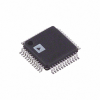
ADUC7032BSTZ-8L-RL Analog Devices Inc, ADUC7032BSTZ-8L-RL Datasheet - Page 104

ADUC7032BSTZ-8L-RL
Manufacturer Part Number
ADUC7032BSTZ-8L-RL
Description
IC,Battery Management,QFP,48PIN,PLASTIC
Manufacturer
Analog Devices Inc
Series
MicroConverter® ADuC7xxxr
Datasheet
1.EVAL-ADUC7032QSPZ.pdf
(116 pages)
Specifications of ADUC7032BSTZ-8L-RL
Core Processor
ARM7
Core Size
16/32-Bit
Speed
20.48MHz
Connectivity
LIN, SPI, UART/USART
Peripherals
POR, PSM, Temp Sensor, WDT
Number Of I /o
9
Program Memory Size
96KB (96K x 8)
Program Memory Type
FLASH
Ram Size
6K x 8
Voltage - Supply (vcc/vdd)
3.5 V ~ 18 V
Data Converters
A/D 2x16b
Oscillator Type
Internal
Operating Temperature
-40°C ~ 105°C
Package / Case
48-LQFP
Lead Free Status / RoHS Status
Lead free / RoHS Compliant
Eeprom Size
-
Lead Free Status / Rohs Status
Compliant
ADuC7032-8L
LIN Hardware Synchronization Control Register 0
Name: LHSCON0
Address: 0xFFFF0784
Default Value: 0x0000
Access: Read/write
Function: This LHS control register is a 16-bit register that, in conjunction with the LHSCON1 register, is used to configure the LIN
mode of operation.
Table 92. LHSCON0 MMR Bit Designations
Bit
15 to 12
11
10
9
8
7
6 to 5
4
3
2
1
0
Description
Reserved. These bits are reserved for future use and should be written as 0 by user software.
Break Timer Compare Interrupt Disable.
Break Timer Error Interrupt Disable.
LIN Transceiver, Standalone Test Mode.
Gate UART Bit.
Sync Timer Stop Edge Type Bit.
Reserved. These bits are reserved for future use and should be written as 0 by user software.
Enable Stop Interrupt.
Enable Start Interrupt.
LIN Sync Enable Bit.
Edge Counter Clear Bit.
LHS Reset Bit.
Set to 1 to disable the break timer compare interrupt.
Cleared to 0 to enable the break timer compare interrupt.
Set to 1 to disable the break timer error interrupt.
Cleared to 0 to enable the break timer error interrupt.
Cleared to 0 by user code to operate the LIN in normal mode, driven directly from the on-chip UART.
Set to 1 by user code to enable external GPIO_7 and GPIO_8 pins to drive the LIN transceiver TxD and RxD, respectively,
independent of the UART. The functions of GPIO_7 and GPIO_8 should first be configured by user code via
GPIO Function Select Bit 0 and GPIO Function Select Bit 4 in the GP2CON register.
Set to 1 by user code to disable the internal UART RxD (receive data) by gating it high until both the break field and
subsequent LIN sync byte have been detected. This ensures the UART does not receive any spurious serial data during break
or sync field periods that need to be flushed out of the UART before valid data fields can be received.
Set to 0 by user code to enable the internal UART RxD (receive data) after the break field and subsequent LIN sync byte have
been detected so that the UART can receive the subsequent LIN data fields.
Cleared to 0 by user code to stop the sync timer on the falling edge count configured via the LHSCON1[7:4] register.
Set to 1 by user code to stop the sync timer on the rising edge count configured via the LHSCON1[7:4] register.
Cleared to 0 by user code to disable interrupts when a stop condition occurs.
Set to 1 by user code to generate an interrupt when a stop condition occurs.
Cleared to 0 by user code to disable interrupts when a start condition occurs.
Set to 1 by user code to generate an interrupt when a start condition occurs.
Cleared to 0 by user code to disable LHS functionality.
Set to 1 by user code to enable LHS functionality.
Cleared to 0 by user code to enable the rising or falling edge counters to function normally.
Set to 1 by user code to clear the internal edge counters in the LHS peripheral. This bit does not reset to 0 automatically and
requires user code to write 0 to re-enable the edge counters.
Cleared to 0 automatically after 15 μs delay.
Set to 1 by user code to reset all LHS logic to default conditions.
Rev.0 | Page 104 of 116


