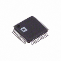
ADUC7032BSTZ-8L-RL Analog Devices Inc, ADUC7032BSTZ-8L-RL Datasheet - Page 44

ADUC7032BSTZ-8L-RL
Manufacturer Part Number
ADUC7032BSTZ-8L-RL
Description
IC,Battery Management,QFP,48PIN,PLASTIC
Manufacturer
Analog Devices Inc
Series
MicroConverter® ADuC7xxxr
Datasheet
1.EVAL-ADUC7032QSPZ.pdf
(116 pages)
Specifications of ADUC7032BSTZ-8L-RL
Core Processor
ARM7
Core Size
16/32-Bit
Speed
20.48MHz
Connectivity
LIN, SPI, UART/USART
Peripherals
POR, PSM, Temp Sensor, WDT
Number Of I /o
9
Program Memory Size
96KB (96K x 8)
Program Memory Type
FLASH
Ram Size
6K x 8
Voltage - Supply (vcc/vdd)
3.5 V ~ 18 V
Data Converters
A/D 2x16b
Oscillator Type
Internal
Operating Temperature
-40°C ~ 105°C
Package / Case
48-LQFP
Lead Free Status / RoHS Status
Lead free / RoHS Compliant
Eeprom Size
-
Lead Free Status / Rohs Status
Compliant
ADuC7032-8L
ADC Mode Register
Name: ADCMDE
Address: 0xFFFF0508
Default Value: 0x00
Access: Read/write
Function: The ADC Mode MMR is an 8-bit register that configures the mode of operation of the ADC subsystem.
Table 36. ADCMDE MMR Bit Designations
Bit
7
6
5
4 to 3
2 to 0
Description
Not Used. This bit is reserved for future functionality and must be written as 0 by user code.
20 kΩ Resistor Select.
Low Power Mode Reference Select.
ADC Power Mode Configuration.
ADC Operation Mode Configuration.
10 = ADC low power plus mode. If enabled, the I-ADC again operates with reduced current consumption. In this mode, the gain
is fixed to 512, and the current consumed is 200 μA (approximately) more than ADC low power mode, shown previously. The
additional current consumed also ensures ADC noise performance is better than that achieved in ADC low power mode.
11 = not defined.
01 = ADC low power mode. If enabled, the I-ADC operates with reduced current consumption. This limitation in current
consumption is achieved (at the expense of ADC noise performance) by fixing the gain to 128 and using the on-chip low power
(131 kHz) oscillator to drive the ADC circuits directly.
Set to 1 to select the 20 kΩ resistor, as shown in Figure 18.
Set to 0 to select the direct path to ground, as shown in Figure 18 (default).
Set to 1 to enable the precision voltage reference in ADC low power mode. This increases current consumption.
Set to 0 to enable the low power voltage reference in ADC low power mode (default).
00 = ADC normal mode. If enabled, the ADC operates with normal current consumption yielding optimum electrical
performance.
000 = ADC power-down mode. All ADC circuits (including internal reference) are powered-down.
001 = ADC continuous conversion mode. In this mode, any enabled ADC continuously converts.
010 = ADC single conversion mode. In this mode, any enabled ADC performs a single conversion. The ADC enters idle mode once the
single-shot conversion is complete. A single conversion takes two to three ADC clock cycles, depending on the chop mode.
011 = ADC idle mode. In this mode, the ADC is fully powered on but is held in r.
100 = ADC self-offset calibration. In this mode, an offset calibration is performed on any enabled ADC using an internally
generated 0 V. The calibration is carried out at the user-programmed ADC settings; therefore, as with a normal single ADC
conversion, it takes two to three ADC conversion cycles before a fully settled calibration result is ready. The calibration result is
automatically written to the ADCxOF MMR of the respective ADC. The ADC returns to idle mode and the calibration- and
conversion-ready status bits are set at the end of an offset calibration cycle.
101 = ADC self-gain calibration. In this mode, a gain calibration against an internal reference voltage is performed on all
enabled ADCs. A gain calibration is a two-stage process that takes twice the time of an offset calibration. The calibration result is
automatically written to the ADCxGN MMR of the respective ADC. The ADC returns to idle mode, and the calibration- and
conversion-ready status bits are set at the end of a gain-calibration cycle. An ADC self-gain calibration should only be carried
out on the current channel ADC, while preprogrammed, factory calibration coefficients (downloaded automatically from internal
Flash) should be used for voltage temperature measurements. If an external NTC is used, an ADC self-calibration should be done
on the temperature channel.
110 = ADC system zero-scale calibration. In this mode, a zero-scale calibration is performed on enabled ADC channels against an
external zero-scale voltage driven at the ADC input pins. The calibration is carried out at the user programmed ADC settings;
therefore, as with a normal single ADC conversion, it takes three ADC conversion cycles before a fully settled calibration result is ready.
111 = ADC system full-scale calibration.
Rev.0 | Page 44 of 116


