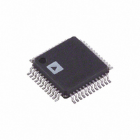
ADUC7032BSTZ-8L-RL Analog Devices Inc, ADUC7032BSTZ-8L-RL Datasheet - Page 102

ADUC7032BSTZ-8L-RL
Manufacturer Part Number
ADUC7032BSTZ-8L-RL
Description
IC,Battery Management,QFP,48PIN,PLASTIC
Manufacturer
Analog Devices Inc
Series
MicroConverter® ADuC7xxxr
Datasheet
1.EVAL-ADUC7032QSPZ.pdf
(116 pages)
Specifications of ADUC7032BSTZ-8L-RL
Core Processor
ARM7
Core Size
16/32-Bit
Speed
20.48MHz
Connectivity
LIN, SPI, UART/USART
Peripherals
POR, PSM, Temp Sensor, WDT
Number Of I /o
9
Program Memory Size
96KB (96K x 8)
Program Memory Type
FLASH
Ram Size
6K x 8
Voltage - Supply (vcc/vdd)
3.5 V ~ 18 V
Data Converters
A/D 2x16b
Oscillator Type
Internal
Operating Temperature
-40°C ~ 105°C
Package / Case
48-LQFP
Lead Free Status / RoHS Status
Lead free / RoHS Compliant
Eeprom Size
-
Lead Free Status / Rohs Status
Compliant
ADuC7032-8L
LIN (LOCAL INTERCONNECT NETWORK) INTERFACE
The ADuC7032-8L features a high voltage physical interface
between the ARM7 MCU core and an external LIN bus. The LIN
interface operates as a slave-only interface operating from 1 kBaud
to 20 kBaud and is compatible with the LIN 2.0 standard. The pull-
up resistor required for a slave node is on-chip, reducing the need
for external circuitry. The LIN protocol is emulated using the
on-chip UART, an IRQ, a dedicated LIN timer, and the high
voltage transceiver, which is also incorporated on-chip. This
emulation is shown in Figure 38. The LIN is clocked from the
low power oscillator, for the break timer; and a 5 MHz output from
the PLL, which is used for the sync byte timing.
GP2DAT[29]
GP2DAT[21]
GPIO_12
131kHz
LHS INTERRUPT
5MHz
AND
IRQEN[7]
ADuC7032-8L
ADuC7032-8L
HARDWARE
UART
LHSVAL0
LHSVAL1
LHS
RxD ENABLE
LHSCON0[8]
GP2CON[20]
FUNCTION
RxD
TxD
GPIO_12
SELECT
INTERRUPT
LOGIC
LHS
DISABLE
OUTPUT
Figure 38. LIN I/O, Block Diagram
SHORT-CIRCUIT
HVCFG0[1:0]
LIN MODE
HVCFG1[2]
CONTROL
FOUR LIN
INTERRUPT
SOURCES
BREAK LHSSTA[0]
START LHSSTA[1]
STOP LHSSTA[2]
BREAK
ERROR LHSSTA[4]
Rev.0 | Page 102 of 116
INPUT
VOLTAGE
THRESHOLD
REFERENCE
BPF
TRIP REFERENCE
SHORT-CIRCUIT
INTERNAL
LIN MMR DESCRIPTION
The LIN hardware synchronization (LHS) functionality is
controlled using the following five MMRs:
•
•
•
•
•
LHSSTA: status register that contains information flags
describing the current status of the interface
LHSCON0: Control Register 0, which controls configuration
of the LHS timer
LHSCON1: start and stop edge control register that dictates at
which edge of the LIN synchronization byte the LHS starts
or stops counting.
LHSVAL0: 16-bit timer that is controlled by LHSCON0.
LHSVAL1: break timer register.
VDD
OVERVOLTAGE
INTERNAL
SHORT-CIRCUIT
SENSE
RESISTOR
PROTECTION
LIN ENABLE
(INTERNAL
HVCFG0[5]
PULL-UP)
EXTERNAL
IO_VSS
LIN PIN
SCR
VDD
MASTER ECU
PROTECTION
DIODE
MASTER ECU
PULL-UP
C
LOAD


