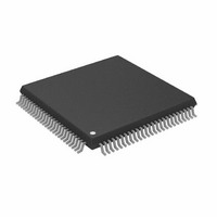
AD8191AASTZ Analog Devices Inc, AD8191AASTZ Datasheet - Page 26

AD8191AASTZ
Manufacturer Part Number
AD8191AASTZ
Description
IC,Telecom Switching Circuit,QFP,100PIN,PLASTIC
Manufacturer
Analog Devices Inc
Datasheet
1.AD8191AASTZ-RL.pdf
(28 pages)
Specifications of AD8191AASTZ
Function
Switch
Circuit
1 x 4:1
On-state Resistance
100 Ohm
Voltage Supply Source
Single Supply
Voltage - Supply, Single/dual (±)
3 V ~ 3.6 V
Operating Temperature
-40°C ~ 85°C
Mounting Type
Surface Mount
Package / Case
100-LQFP
Lead Free Status / RoHS Status
Lead free / RoHS Compliant
Available stocks
Company
Part Number
Manufacturer
Quantity
Price
Company:
Part Number:
AD8191AASTZ
Manufacturer:
Analog Devices Inc
Quantity:
10 000
Company:
Part Number:
AD8191AASTZ-RL
Manufacturer:
Analog Devices Inc
Quantity:
10 000
AD8191A
Power Supplies
The AD8191A has five separate power supplies referenced to
two separate grounds. The supply/ground pairs are:
•
•
•
•
•
The AVCC/AVEE (3.3 V) and DVCC/DVEE (3.3 V) supplies
power the core of the AD8191A. The VTTI/AVEE supply
(3.3 V) powers the input termination (see Figure 25). Similarly,
the VTTO/AVEE supply (3.3 V) powers the output termination
(see Figure 26). The AMUXVCC/DVEE supply (3.3 V to 5 V)
powers the auxiliary multiplexer core and determines the
maximum allowed voltage on the auxiliary lines. For example,
if the DDC bus is using 5 V I
to 5 V relative to DVEE.
In a typical application, all pins labeled AVEE or DVEE should
be connected directly to ground. All pins labeled AVCC,
DVCC, VTTI, or VTTO should be connected to 3.3 V, and
Pin AMUXVCC tied to 5 V. The supplies can also be powered
individually, but care must be taken to ensure that each stage of
the AD8191A is powered correctly.
Power Supply Bypassing
The AD8191A requires minimal supply bypassing. When
powering the supplies individually, place a 0.01 μF capacitor
between each 3.3 V supply pin (AVCC, DVCC, VTTI, and
VTTO) and ground to filter out supply noise. Generally, bypass
capacitors should be placed near the power pins and should
connect directly to the relevant supplies (without long intervening
traces). For example, to improve the parasitic inductance of the
power supply decoupling capacitors, minimize the trace length
between capacitor landing pads and the vias, as shown in Figure 34.
AVCC/AVEE
VTTI/AVEE
VTTO/AVEE
DVCC/DVEE
AMUXVCC/DVEE
2
C, AMUXVCC should be connected
Rev. 0 | Page 26 of 28
In applications where the AD8191A is powered by a single 3.3 V
supply, it is recommended to use two reference supply planes
and bypass the 3.3 V reference plane to the ground reference
plane with one 220 pF capacitor, one 1000 pF capacitor, two
0.01 μF capacitors, and one 4.7 μF capacitor. The capacitors
should via down directly to the supply planes and be placed
within a few centimeters of the AD8191A. The AMUXVCC
supply does not require additional bypassing. This bypassing
scheme is illustrated in Figure 35.
AUXILIARY LINES
TMDS TRACES
Figure 34. Recommended Pad Outline for Bypass Capacitors
Figure 35. Example Placement of Power Supply
Decoupling Capacitors Around the AD8191A
AD8191A
RECOMMENDED
NOT RECOMMENDED
EXTRA ADDED INDUCTANCE
DECOUPLING
CAPACITORS


