AD8191AASTZ Analog Devices Inc, AD8191AASTZ Datasheet - Page 2
AD8191AASTZ
Manufacturer Part Number
AD8191AASTZ
Description
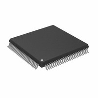
IC,Telecom Switching Circuit,QFP,100PIN,PLASTIC
Manufacturer
Analog Devices Inc
Datasheet
1.AD8191AASTZ-RL.pdf
(28 pages)
Specifications of AD8191AASTZ
Function
Switch
Circuit
1 x 4:1
On-state Resistance
100 Ohm
Voltage Supply Source
Single Supply
Voltage - Supply, Single/dual (±)
3 V ~ 3.6 V
Operating Temperature
-40°C ~ 85°C
Mounting Type
Surface Mount
Package / Case
100-LQFP
Lead Free Status / RoHS Status
Lead free / RoHS Compliant
Available stocks
Company
Part Number
Manufacturer
Quantity
Price
Company:

Part Number:
AD8191AASTZ
Manufacturer:
Analog Devices Inc
Quantity:
10 000
Company:
Part Number:
AD8191AASTZ-RL
Manufacturer:
Analog Devices Inc
Quantity:
10 000


AD8191A
TABLE OF CONTENTS
Features .............................................................................................. 1
Applications....................................................................................... 1
Functional Block Diagram .............................................................. 1
Typical Application........................................................................... 1
General Description ......................................................................... 1
Product Highlights ........................................................................... 1
Revision History ............................................................................... 2
Specifications..................................................................................... 3
Absolute Maximum Ratings............................................................ 5
Pin Configuration and Function Descriptions............................. 6
Typical Performance Characteristics ............................................. 9
Theory of Operation ...................................................................... 13
Serial Control Interface.................................................................. 15
REVISION HISTORY
11/07—Revision 0: Initial Version
Thermal Resistance ...................................................................... 5
Maximum Power Dissipation ..................................................... 5
ESD Caution.................................................................................. 5
Introduction ................................................................................ 13
Input Channels............................................................................ 13
Output Channels ........................................................................ 13
Auxiliary Switch.......................................................................... 14
Reset ............................................................................................. 15
Write Procedure.......................................................................... 15
Read Procedure........................................................................... 16
Rev. 0 | Page 2 of 28
Parallel Control Interface .............................................................. 17
Serial Interface Configuration Registers ..................................... 18
Parallel Interface Configuration Registers .................................. 20
Applications Information .............................................................. 22
Outline Dimensions ....................................................................... 27
Switching/Update Delay............................................................ 16
High Speed Device Modes Register......................................... 18
Auxiliary Device Modes Register............................................. 18
Receiver Settings Register ......................................................... 19
Input Termination Pulse Register 1 and Register 2 ............... 19
Receive Equalizer Register 1 and Register 2 ........................... 19
Transmitter Settings Register.................................................... 19
High Speed Device Modes Register......................................... 20
Auxiliary Device Modes Register............................................. 20
Receiver Settings Register ......................................................... 20
Input Termination Pulse Register 1 and Register 2 ............... 21
Receive Equalizer Register 1 and Register 2 ........................... 21
Transmitter Settings Register.................................................... 21
Pinout........................................................................................... 22
Cable Lengths and Equalization............................................... 23
PCB Layout Guidelines.............................................................. 23
Ordering Guide .......................................................................... 27
Related parts for AD8191AASTZ
Image
Part Number
Description
Manufacturer
Datasheet
Request
R

Part Number:
Description:
BOARD EVAL FOR AD8191 HDMI/DVI
Manufacturer:
Analog Devices Inc
Datasheet:

Part Number:
Description:
SENSOR GAS FOR CO/NO2 EXHAUST
Manufacturer:
GE Sensing
Datasheet:

Part Number:
Description:
±1.7g Dual-Axis IMEMS Accelerometer Evaluation Board
Manufacturer:
Analog Devices Inc
Datasheet:
Part Number:
Description:
Inertial Sensor Evaluation System
Manufacturer:
Analog Devices Inc
Datasheet:
Part Number:
Description:
Manufacturer:
Analog Devices Inc
Datasheet:
Part Number:
Description:
Manufacturer:
Analog Devices Inc
Datasheet:
Part Number:
Description:
Manufacturer:
Analog Devices Inc
Datasheet:
Part Number:
Description:
Manufacturer:
Analog Devices Inc
Datasheet:
Part Number:
Description:
Manufacturer:
Analog Devices Inc
Datasheet:
Part Number:
Description:
Manufacturer:
Analog Devices Inc
Datasheet:
Part Number:
Description:
Manufacturer:
Analog Devices Inc
Datasheet:
Part Number:
Description:
Manufacturer:
Analog Devices Inc
Datasheet:
Part Number:
Description:
Manufacturer:
Analog Devices Inc
Datasheet: