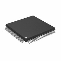
AD8191AASTZ Analog Devices Inc, AD8191AASTZ Datasheet - Page 22

AD8191AASTZ
Manufacturer Part Number
AD8191AASTZ
Description
IC,Telecom Switching Circuit,QFP,100PIN,PLASTIC
Manufacturer
Analog Devices Inc
Datasheet
1.AD8191AASTZ-RL.pdf
(28 pages)
Specifications of AD8191AASTZ
Function
Switch
Circuit
1 x 4:1
On-state Resistance
100 Ohm
Voltage Supply Source
Single Supply
Voltage - Supply, Single/dual (±)
3 V ~ 3.6 V
Operating Temperature
-40°C ~ 85°C
Mounting Type
Surface Mount
Package / Case
100-LQFP
Lead Free Status / RoHS Status
Lead free / RoHS Compliant
Available stocks
Company
Part Number
Manufacturer
Quantity
Price
Company:
Part Number:
AD8191AASTZ
Manufacturer:
Analog Devices Inc
Quantity:
10 000
Company:
Part Number:
AD8191AASTZ-RL
Manufacturer:
Analog Devices Inc
Quantity:
10 000
AD8191A
APPLICATIONS INFORMATION
The AD8191A is an HDMI/DVI switch featuring equalized
TMDS inputs and pre-emphasized TMDS outputs. It is intended
for use as a 4:1 switch in systems with long cable runs on both
the input and/or the output and is fully HDMI 1.2a receive-
compliant.
PINOUT
The AD8191A is designed to have an HDMI/DVI receiver
pinout at its input and a transmitter pinout at its output, which
makes the AD8191A ideal for use in AVR-type applications
where a designer routes both the inputs and the outputs directly
to HDMI/DVI connectors. This type of layout is used on the
AD8191A evaluation board, as shown in Figure 31. When the
AD8191A is used in receiver type applications, it is necessary to
change the order of the output pins on the PCB to align with the
on-board receiver.
One advantage of the AD8191A in an AVR-type application is
that all of the high speed signals can be routed on one side (the
topside) of the board, as shown in Figure 31. In addition to 12 dB of
input equalization, the AD8191A provides up to 6 dB of output
pre-emphasis that boosts the output TMDS signals and allows
the AD8191A to precompensate when driving long
Figure 31. Layout of the TMDS Traces on the AD8191A Evaluation Board (Only Top Signal Routing Layer is Shown)
Rev. 0 | Page 22 of 28
PCB traces or output cables. The net effect of the input
equalization and output pre-emphasis of the AD8191A is that
the AD8191A can compensate for the signal degradation of
both input and output cables; it acts to reopen a closed input
data eye and transmits a full-swing HDMI signal to an end
receiver.
The AD8191A also provides a distinct advantage in receive-type
applications because it is a fully buffered HDMI/DVI switch.
Although inverting the output pin order of the AD8191A on the
PCB requires a designer to place vias in the high speed signal
path, the AD8191A fully buffers and electrically decouples the
outputs from the inputs. Consequently, the effects of the vias
placed on the output signal lines are not seen at the input of the
AD8191A. The programmable output terminations also improve
signal quality at the output of the AD8191A. Therefore, the PCB
designer has significantly improved flexibility in the placement
and routing of the output signal path with the AD8191A over
other solutions.


