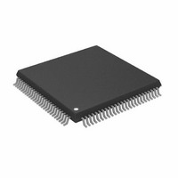
AD8191AASTZ Analog Devices Inc, AD8191AASTZ Datasheet - Page 23

AD8191AASTZ
Manufacturer Part Number
AD8191AASTZ
Description
IC,Telecom Switching Circuit,QFP,100PIN,PLASTIC
Manufacturer
Analog Devices Inc
Datasheet
1.AD8191AASTZ-RL.pdf
(28 pages)
Specifications of AD8191AASTZ
Function
Switch
Circuit
1 x 4:1
On-state Resistance
100 Ohm
Voltage Supply Source
Single Supply
Voltage - Supply, Single/dual (±)
3 V ~ 3.6 V
Operating Temperature
-40°C ~ 85°C
Mounting Type
Surface Mount
Package / Case
100-LQFP
Lead Free Status / RoHS Status
Lead free / RoHS Compliant
Available stocks
Company
Part Number
Manufacturer
Quantity
Price
Company:
Part Number:
AD8191AASTZ
Manufacturer:
Analog Devices Inc
Quantity:
10 000
Company:
Part Number:
AD8191AASTZ-RL
Manufacturer:
Analog Devices Inc
Quantity:
10 000
CABLE LENGTHS AND EQUALIZATION
The AD8191A offers two levels of programmable equalization
for the high speed inputs: 6 dB and 12 dB. The equalizer of the
AD8191A supports video data rates of 1.65 Gbps. It can
equalize up to 20 meters of 24 AWG HDMI cable at data rates
corresponding to the video format, 1080p.
The length of cable that can be used in a typical HDMI/DVI
application depends on a large number of factors, including:
•
•
•
•
As such, specific cable types and lengths are not recommended
for use with a particular equalizer setting. In nearly all applica-
tions, the AD8191A equalization level can be set to high, or 12 dB,
for all input cable configurations at all data rates, without degrading
the signal integrity.
PCB LAYOUT GUIDELINES
The AD8191A is used to switch two distinctly different types
of signals, both of which are required for HDMI and DVI video.
These signal groups require different treatment when laying
out a PCB.
The first group of signals carries the audiovisual (AV) data. HDMI/
DVI video signals are differential, unidirectional, and high speed
(up to 1.65 Gbps). The channels that carry the video data must
be controlled impedance, terminated at the receiver, and capable
of operating up to at least 1.65 Gbps. It is especially important
to note that the differential traces that carry the TMDS signals
should be designed with a controlled differential impedance of
100 Ω. The AD8191A provides single-ended, 50 Ω terminations
on-chip for both its inputs and outputs, and both the input and
output terminations can be enabled or disabled through the
serial interface. Transmitter termination is not fully specified by
the HDMI standard but its inclusion improves the overall system
signal integrity.
The audiovisual data carried on these high speed channels are
encoded by a technique called transmission minimized differential
signaling (TMDS) and, in the case of HDMI, is also encrypted
according to the high bandwidth digital copy protection (HDCP)
standard.
Cable quality: the quality of the cable in terms of conductor
wire gauge and shielding. Thicker conductors have lower
signal degradation per unit length.
Data rate: the data rate being sent over the cable. The signal
degradation of HDMI cables increases with data rate.
Edge rates: the edge rates of the source input. Slower input
edges result in more significant data eye closure at the end
of a cable.
Receiver sensitivity: the sensitivity of the terminating
receiver.
Rev. 0 | Page 23 of 28
The second group of signals consists of low speed auxiliary
control signals used for communication between a source and a
sink. Depending upon the application, these signals can include
the DDC bus (an I
HDCP encryption keys between the source and the sink), the
consumer electronics control (CEC) line, and the hot plug
detect (HPD) line. These auxiliary signals are bidirectional, low
speed, and transferred over a single-ended transmission line
that does not need to have controlled impedance. The primary
concern with laying out the auxiliary lines is ensuring that they
conform to the I
capacitive loading.
TMDS Signals
In the HDMI/DVI standard, four differential pairs carry the
TMDS signals. In DVI, three of these pairs are dedicated to
carrying RGB video and sync data. For HDMI, audio data is
interleaved with the video data; the DVI standard does not
incorporate audio information. The fourth high speed differential
pair is used for the AV data-word clock and runs at one-tenth
the speed of the TMDS data channels.
The four high speed channels of the AD8191A are identical.
No concession was made to lower the bandwidth of the fourth
channel for the pixel clock; therefore, any channel can be used
for any TMDS signal. The user chooses which signal is routed
over which channel. Additionally, the TMDS channels are
symmetrical; therefore, the p and n of a given differential pair
are interchangeable, provided the inversion is consistent across
all inputs and outputs of the AD8191A. However, the routing
between inputs and outputs through the AD8191A is fixed.
The AD8191A buffers the TMDS signals and the input traces
can be considered electrically independent of the output traces.
In most applications, the quality of the signal on the input TMDS
traces is more sensitive to the PCB layout. Regardless of the data
being carried on a specific TMDS channel, or whether the TMDS
line is at the input or the output of the AD8191A, all four high
speed signals should be routed on a PCB in accordance with the
same RF layout guidelines.
Layout for the TMDS Signals
The TMDS differential pairs can be either microstrip traces,
routed on the outer layer of a board, or stripline traces, routed
on an internal layer of the board. If microstrip traces are used,
there should be a continuous reference plane on the PCB layer
directly below the traces. If stripline traces are used, they must
be sandwiched between two continuous reference planes in the
PCB stack-up.
2
C bus standard and do not have excessive
2
C bus used to send EDID information and
AD8191A


