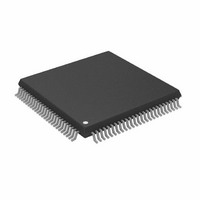
AD8191AASTZ Analog Devices Inc, AD8191AASTZ Datasheet - Page 13

AD8191AASTZ
Manufacturer Part Number
AD8191AASTZ
Description
IC,Telecom Switching Circuit,QFP,100PIN,PLASTIC
Manufacturer
Analog Devices Inc
Datasheet
1.AD8191AASTZ-RL.pdf
(28 pages)
Specifications of AD8191AASTZ
Function
Switch
Circuit
1 x 4:1
On-state Resistance
100 Ohm
Voltage Supply Source
Single Supply
Voltage - Supply, Single/dual (±)
3 V ~ 3.6 V
Operating Temperature
-40°C ~ 85°C
Mounting Type
Surface Mount
Package / Case
100-LQFP
Lead Free Status / RoHS Status
Lead free / RoHS Compliant
Available stocks
Company
Part Number
Manufacturer
Quantity
Price
Company:
Part Number:
AD8191AASTZ
Manufacturer:
Analog Devices Inc
Quantity:
10 000
Company:
Part Number:
AD8191AASTZ-RL
Manufacturer:
Analog Devices Inc
Quantity:
10 000
THEORY OF OPERATION
INTRODUCTION
The primary function of the AD8191A is to switch one of four
(HDMI or DVI) single-link sources to one output. Each HDMI/
DVI link consists of four differential, high speed channels and
four auxiliary single-ended, low speed control signals. The high
speed channels include a data-word clock and three transition
minimized differential signaling (TMDS) data channels running at
10× the data-word clock frequency for data rates up to 1.65 Gbps.
The four low speed control signals are 5 V tolerant bidirectional
lines that can carry configuration signals, HDCP encryption, and
other information, depending upon the specific application.
All four high speed TMDS channels in a given link are identical;
that is, the pixel clock can be run on any of the four TMDS
channels. Transmit and receive channel compensation is provided
for the high speed channels where the user can (manually)
select among a number of fixed settings.
The AD8191A has two control interfaces. Users have the option
of controlling the part through either the parallel control interface
or the I
programmable I
to be controlled by a single I
restore the control registers of the AD8191A to default values.
In all cases, serial programming values override any prior parallel
programming values, and any use of the serial control interface
disables the parallel control interface until the AD8191A is reset.
INPUT CHANNELS
Each high speed input differential pair terminates to the 3.3 V
VTTI power supply through a pair of single-ended 50 Ω on-chip
resistors, as shown in Figure 25. The input terminations can be
optionally disconnected for approximately 100 ms following a
source switch. The user can program which of the 16 high speed
input channels employs this feature by selectively programming
the associated RX_PT bits in the input termination pulse registers
through the serial control interface. Additionally, all the input
terminations can be disconnected by programming the RX_TO
bit in the receiver settings register. By default, the input termination
is enabled. The input terminations are enabled and cannot be
switched when programming the AD8191A through the parallel
control interface.
2
C serial control interface. The AD8191A has eight user-
IN_xx
IP_xx
Figure 25. High Speed Input Simplified Schematic
2
C slave addresses to allow multiple AD8191As
AVEE
VTTI
2
C bus. A RESET pin is provided to
50Ω
50Ω
CABLE
EQ
Rev. 0 | Page 13 of 28
The input equalizer can be manually configured to provide two
different levels of high frequency boost: 6 dB or 12 dB. The user
can individually control the equalization level of the eight high
speed input channels by selectively programming the associated
RX_EQ bits in the receive equalizer register through the serial
control interface. Alternately, the user can globally control the
equalization level of all eight high speed input channels by setting
the PP_EQ pin of the parallel control interface. No specific
cable length is suggested for a particular equalization setting
because cable performance varies widely between manufacturers;
however, in general, the equalization of the AD8191A can be set
to 12 dB without degrading the signal integrity, even for short
input cables. At the 12 dB setting, the AD8191A can equalize
more than 20 meters of 24 AWG cable at 1.65 Gbps.
OUTPUT CHANNELS
Each high speed output differential pair is terminated to the
3.3 V VTTO power supply through a 50 Ω on-chip resistor (see
Figure 26). This termination is user-selectable; it can be turned
on or off by programming the TX_PTO bit of the transmitter
settings register through the serial control interface, or by
setting the PP_OTO pin of the parallel control interface.
The output termination resistors of the AD8191A back-terminate
the output TMDS transmission lines. These back-terminations
act to absorb reflections from impedance discontinuities on the
output traces, improving the signal integrity of the output traces
and adding flexibility to how the output traces can be routed.
For example, interlayer vias can be used to route the AD8191A
TMDS outputs on multiple layers of the PCB without severely
degrading the quality of the output signal.
The AD8191A output has a disable feature that places the
outputs in a tristate mode. This mode is enabled by programming
the HS_EN bit of the high speed device modes register through
the serial control interface or by setting the PP_EN pin of the
parallel control interface. Larger wire-OR’ e d arrays can be
constructed using the AD8191A in this mode.
Figure 26. High Speed Output Simplified Schematic
OPx
DISABLE
50Ω
VTTO
AVEE
I
OUT
50Ω
ONx
AD8191A


