SI4310BDY-T1-E3 Vishay, SI4310BDY-T1-E3 Datasheet - Page 2
SI4310BDY-T1-E3
Manufacturer Part Number
SI4310BDY-T1-E3
Description
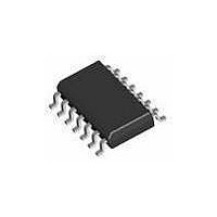
TRANSISTOR,MOSFET,MATCHED PAIR,N-CHANNEL,30V V(BR)DSS,9.8A I(D),SO
Manufacturer
Vishay
Datasheet
1.SI4310BDY-T1-E3.pdf
(10 pages)
Specifications of SI4310BDY-T1-E3
Minimum Operating Temperature
- 55 C
Configuration
Dual
Transistor Polarity
N-Channel
Resistance Drain-source Rds (on)
0.011 Ohm @ 10 V @ Channel 1
Drain-source Breakdown Voltage
30 V
Gate-source Breakdown Voltage
+/- 20 V
Continuous Drain Current
7.5 A @ Channel 1 or 9.8 A @ Channel 2
Power Dissipation
1140 mW @ Channel 1 or 1470 mW @ Channel 2
Maximum Operating Temperature
+ 150 C
Mounting Style
SMD/SMT
Package / Case
SOIC-8 Narrow
Lead Free Status / RoHS Status
Lead free / RoHS Compliant
Lead Free Status / RoHS Status
Lead free / RoHS Compliant


Si4310BDY
Vishay Siliconix
Notes:
a. Guaranteed by design, not subject to production testing.
b. Pulse test; pulse width ≤ 300 µs, duty cycle ≤ 2 %.
www.vishay.com
2
MOSFET SPECIFICATIONS T
Parameter
Static
Gate Threshold Voltage
Gate-Body Leakage
Zero Gate Voltage Drain Current
On-State Drain Current
Drain-Source On-State Resistance
Forward Transconductance
Diode Forward Voltage
Dynamic
Input Capacitance
Output Capacitance
Reverse Transfer Capacitance
Total Gate Charge
Gate-Source Charge
Gate-Drain Charge
Gate Resistance
Turn-On Delay Time
Rise Time
Turn-Off Delay Time
Fall Time
Source-Drain Reverse Recovery Time
a
b
b
b
b
J
= 25 °C, unless otherwise noted
Symbol
R
V
I
t
t
I
I
C
DS(on)
V
C
GS(th)
D(on)
C
Q
Q
d(on)
d(off)
GSS
DSS
g
Q
R
t
SD
oss
t
t
rss
iss
rr
fs
gs
gd
r
f
g
g
V
V
V
V
I
I
DS
DS
DS
D
D
DS
I
I
≅ 1 A, V
≅ 1 A, V
F
F
= 15 V, V
= 15 V, V
V
= 30 V, V
V
= 15 V, V
= 2.73 V, dI/dt = 100 A/µs
V
V
V
V
V
= 1.8 A, dI/dt = 100 A/µs
V
I
DS
V
V
V
V
DS
I
S
GS
S
DD
DD
DS
DS
GS
GS
GS
DS
DS
= 2.73 V, V
= 1.8 V, V
= 0 V, V
= V
= 4.5 V, I
= 30 V, V
= 5 V, V
= 15 V, R
= 15 V, R
= 4.5 V, I
= 10 V, I
= 10 V, I
= 15 V, I
= 15 V, I
Channel-1
Channel-2
Channel-1
GEN
Channel-2
GEN
f = 1 MHz
Test Conditions
GS
GS
GS
GS
GS
, I
= 10 V, R
= 10 V, R
= 4.5 V, I
= 4.5 V, I
= 0 V, T
GS
= 0 V, f = 1 MHz
D
GS
GS
D
D
D
D
D
= 250 µA
GS
D
GS
L
L
= ± 20 V
= 10 A
= 14 A
= 8.2 A
= 10 A
= 14 A
= 13 A
= 15 Ω
= 15 Ω
= 10 V
= 0 V
= 0 V
= 0 V
J
D
D
g
g
= 85 °C
= 6 Ω
= 6 Ω
= 10 A
= 14 A
Ch-1
Ch-2
Ch-1
Ch-2
Ch-1
Ch-2
Ch-1
Ch-2
Ch-1
Ch-2
Ch-1
Ch-2
Ch-1
Ch-2
Ch-1
Ch-2
Ch-1
Ch-2
Ch-1
Ch-2
Ch-1
Ch-2
Ch-1
Ch-2
Ch-1
Ch-2
Ch-1
Ch-2
Ch-1
Ch-2
Ch-1
Ch-2
Ch-1
Ch-2
Ch-1
Ch-2
Ch-1
Ch-2
Ch-1
Ch-2
Ch-1
Ch-2
1530
Min.
0.90
790
145
300
115
1.0
1.0
0.3
70
20
30
S09-2436-Rev. B, 16-Nov-09
Document Number: 73064
0.0065 0.0085
0.0075 0.0095
Typ.
0.009
0.013
0.485
1580
3060
0.76
0.95
290
600
140
225
5.3
4.3
1.8
30
60
12
19
10
13
17
10
12
33
53
10
17
25
31
5
a
0.011
0.016
Max.
4000
2370
4590
0.53
100
100
100
435
900
210
340
3.0
3.0
1.1
2.7
1.4
15
18
30
20
26
15
20
50
80
15
26
40
50
1
Unit
µA
nC
nA
pF
ns
V
A
Ω
S
V
Ω
Related parts for SI4310BDY-T1-E3
Image
Part Number
Description
Manufacturer
Datasheet
Request
R

Part Number:
Description:
Dual N-Channel 30-V (D-S) MOSFET with Schottky Diode
Manufacturer:
VISHAY [Vishay Siliconix]
Datasheet:

Part Number:
Description:
Dual N-channel 30-v D-s Mosfet With Schottky Diode
Manufacturer:
Vishay
Datasheet:
Part Number:
Description:
357-036-542-201 CARDEDGE 36POS DL .156 BLK LOPRO
Manufacturer:
Vishay
Datasheet:
Part Number:
Description:
357-036-542-201 CARDEDGE 36POS DL .156 BLK LOPRO
Manufacturer:
Vishay
Datasheet:
Part Number:
Description:
357-036-542-201 CARDEDGE 36POS DL .156 BLK LOPRO
Manufacturer:
Vishay
Datasheet:
Part Number:
Description:
357-036-542-201 CARDEDGE 36POS DL .156 BLK LOPRO
Manufacturer:
Vishay
Datasheet:
Part Number:
Description:
357-036-542-201 CARDEDGE 36POS DL .156 BLK LOPRO
Manufacturer:
Vishay
Datasheet:
Part Number:
Description:
357-036-542-201 CARDEDGE 36POS DL .156 BLK LOPRO
Manufacturer:
Vishay
Datasheet:
Part Number:
Description:
357-036-542-201 CARDEDGE 36POS DL .156 BLK LOPRO
Manufacturer:
Vishay
Datasheet:
Part Number:
Description:
357-036-542-201 CARDEDGE 36POS DL .156 BLK LOPRO
Manufacturer:
Vishay
Datasheet:
Part Number:
Description:
357-036-542-201 CARDEDGE 36POS DL .156 BLK LOPRO
Manufacturer:
Vishay
Datasheet:
Part Number:
Description:
357-036-542-201 CARDEDGE 36POS DL .156 BLK LOPRO
Manufacturer:
Vishay
Datasheet:
Part Number:
Description:
357-036-542-201 CARDEDGE 36POS DL .156 BLK LOPRO
Manufacturer:
Vishay
Datasheet:
Part Number:
Description:
357-036-542-201 CARDEDGE 36POS DL .156 BLK LOPRO
Manufacturer:
Vishay
Datasheet:
Part Number:
Description:
357-036-542-201 CARDEDGE 36POS DL .156 BLK LOPRO
Manufacturer:
Vishay
Datasheet: