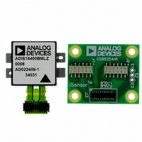
ADIS16400/PCBZ Analog Devices Inc, ADIS16400/PCBZ Datasheet - Page 12
ADIS16400/PCBZ
Manufacturer Part Number
ADIS16400/PCBZ
Description
ADIS16400/PCB EVAL. BD. PB Free
Manufacturer
Analog Devices Inc
Series
iMEMS®, iSensor™r
Specifications of ADIS16400/PCBZ
Sensor Type
Accelerometer, Gyroscope, Magnetometer, 3 Axis
Sensing Range
±18g, ±75°/sec, ±150°/sec, ±300°/sec, ±2.5gauss
Interface
SPI Serial
Sensitivity
3.33mg/LSB, 0.0125 ~ 0.05°/sec/LSB, 0.5mgauss/LSB
Voltage - Supply
4.75 V ~ 5.25 V
Embedded
No
Utilized Ic / Part
ADIS16400
Silicon Manufacturer
Analog Devices
Silicon Core Number
ADIS16400
Kit Application Type
Sensing - Navigation / Position
Application Sub Type
Accelerometer / Gyroscope
Kit Contents
Board, Manual
Rohs Compliant
Yes
Lead Free Status / RoHS Status
Lead free / RoHS Compliant


ADIS16400/ADIS16405
OUTPUT DATA REGISTERS
Figure 6 provides the positive measurement direction for each
gyroscope, accelerometer, and magnetometer. Table 9 provides
the configuration and scale factor for each output data register
in the ADIS16400/ADIS16405. All inertial sensor outputs are in
14-bit, twos complement format, which means that 0x0000 is
equal to 0 LSB, 0x0001 is equal to +1 LSB, and 0x3FFF is equal to
−1 LSB. The following is an example of how to calculate the
sensor measurement from the XGYRO_OUT:
Therefore, an XGYRO_OUT output of 0x3B4A corresponds to
a clockwise rotation about the z-axis (see Figure 6) of 60.3°/sec
when looking at the top of the package.
Table 9. Output Data Register Formats
Register
SUPPLY_OUT
XGYRO_OUT
YGYRO_OUT
ZGYRO_OUT
XACCL_OUT
YACCL_OUT
ZACCL_OUT
XMAGN_OUT
YMAGN_OUT
ZMAGN_OUT
TEMP_OUT
AUX_ADC
1
2
Each output data register uses the bit assignments shown in
Figure 13. The ND flag indicates that unread data resides in the
output data registers. This flag clears and returns to 0 during an
output register read sequence. It returns to 1 after the next internal
sample updates the registers with new data. The EA flag indicates
that one of the error flags in the DIAG_STAT register (see Table 23)
is active (true). The remaining 14 bits are for data.
Assumes that the scaling is set to ±300°/sec. This factor scales with the range.
The typical output for this register at 25°C is 0x0000.
XGYRO_OUT = 0x3B4A
0x000 − 0x3B4A = −0x04B6 = (4 × 256 + 11 × 16 + 6) −
Rate = 0.05°/sec × (−1206) = −60.3°/sec
0x04B6 = −1206 LSB
ND EA
2
DOUT
1
1
SCLK
1
DIN
Figure 13. Output Register Bit Assignments
CS
Bits
14
14
14
14
14
14
14
14
14
14
12
12
PREVIOUS
0x3E00
Format
Binary, 5 V = 0x0814
Twos complement
Twos complement
Twos complement
Twos complement
Twos complement
Twos complement
Twos complement
Twos complement
Twos complement
Twos complement
Binary, 1 V = 0x04D9
MSB FOR 14-BIT OUTPUT
1
MSB FOR 12-BIT OUTPUT
SUPPLY_OUT
DON’T CARE
2
Scale
2.418 mV
0.05°/sec
0.05°/sec
0.05°/sec
3.33 mg
3.33 mg
3.33 mg
0.5 mgauss
0.5 mgauss
0.5 mgauss
0.14°C
806 μV
Figure 12. Burst Mode Read Sequence
XGYRO_OUT
Rev. B | Page 12 of 20
3
YGYRO_OUT
Auxiliary ADC
The AUX_ADC register provides access to the auxiliary ADC
input channel. The ADC is a 12-bit successive approximation
converter that has an equivalent input circuit to the one shown
in Figure 14. The maximum input is 3.3 V. The ESD protection
diodes can handle 10 mA without causing irreversible damage.
The on resistance (R1) of the switch has a typical value of 100 Ω.
The sampling capacitor, C2, has a typical value of 16 pF.
CALIBRATION
Manual Bias Calibration
The bias offset registers in Table 10, Table 11, and Table 12
(hard-iron correction for magnetometer) provide a manual
adjustment function for the output of each sensor. For example,
if XGYRO_OFF equals 0x1FF6, the XGYRO_OUT offset shifts
by −10 LSB, or −0.125°/sec. The DIN command for the upper
byte is DIN = 0x9B1F; for the lower byte, DIN = 0x9AF6.
Table 10. XGYRO_OFF, YGYRO_OFF, ZGYRO_OFF
Bits
[15:13]
[12:0]
Table 11. XACCL_OFF, YACCL_OFF, ZACCL_OFF
Bits
[15:12]
[11:0]
Table 12. XMAGN_HIF, YMAGN_HIF, ZMAGN_HIF
Bits
[15:14]
[13:0]
4
(Conversion Phase: Switch Open, Track Phase: Switch Closed)
Description
Not used.
Data bits. Twos complement, 0.0125°/sec per LSB.
Typical adjustment range = ±50°/sec.
Description
Not used.
Data bits. Twos complement, 3.3 mg/LSB.
Typical adjustment range = ±6.75 g.
Description
Not used.
Data bits. Twos complement, 0.5 mgauss/LSB.
Typical adjustment range = ±4 gauss.
Figure 14. Equivalent Analog Input Circuit
ZGYRO_OUT
C1
5
VCC
D
D
R1
AUX_ADC
C2
13
Default = 0x0000
Default = 0x0000
Default = 0x0000
Related parts for ADIS16400/PCBZ
Image
Part Number
Description
Manufacturer
Datasheet
Request
R

Part Number:
Description:
±1.7g Dual-Axis IMEMS Accelerometer Evaluation Board
Manufacturer:
Analog Devices Inc
Datasheet:

Part Number:
Description:
Inertial Sensor Evaluation System
Manufacturer:
Analog Devices Inc
Datasheet:
Part Number:
Description:
Manufacturer:
Analog Devices Inc
Datasheet:
Part Number:
Description:
Manufacturer:
Analog Devices Inc
Datasheet:
Part Number:
Description:
Manufacturer:
Analog Devices Inc
Datasheet:
Part Number:
Description:
Manufacturer:
Analog Devices Inc
Datasheet:
Part Number:
Description:
Manufacturer:
Analog Devices Inc
Datasheet:
Part Number:
Description:
Manufacturer:
Analog Devices Inc
Datasheet:
Part Number:
Description:
Manufacturer:
Analog Devices Inc
Datasheet:
Part Number:
Description:
Manufacturer:
Analog Devices Inc
Datasheet:
Part Number:
Description:
Manufacturer:
Analog Devices Inc
Datasheet:
Part Number:
Description:
Manufacturer:
Analog Devices Inc
Datasheet:
Part Number:
Description:
Manufacturer:
Analog Devices Inc
Datasheet: