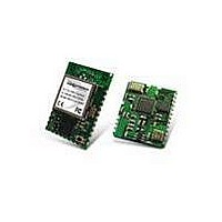
WI.232FHSS-250-R Radiotronix, WI.232FHSS-250-R Datasheet - Page 31

WI.232FHSS-250-R
Manufacturer Part Number
WI.232FHSS-250-R
Description
RF Modules & Development Tools 900MHz FHSS Low
Manufacturer
Radiotronix
Datasheet
1.WI.232FHSS-25-FCC-RA-R.pdf
(67 pages)
Specifications of WI.232FHSS-250-R
Lead Free Status / RoHS Status
Lead free / RoHS Compliant
Other names
WI232FHSS-250-R
- Current page: 31 of 67
- Download datasheet (937Kb)
WI.232FHSS-25-R/ WI.232FHSS-250-R DATASHEET
Table 10, Wi.232FHSS Reset Circuit Specifications
3.6.6. Receive Signal Strength Indication (RSSI)
The RSSI pin contains an analog voltage proportional to the signal strength present on the channel at the
time. In normal operation, the module is hopping rapidly from channel to channel looking for valid data. In
this case, the RSSI value does not provide much in the way of useful information. However, it can be used to
keep a module awake. For instance, if you are preparing to put the module to sleep, you may sample the
RSSI pin to determine if it is processing a packet.
The Wi.232FHSS-250-R module has an internal, digital RSSI indication of
good packet
state of the packet engine.
RSSI level is dependent on the power of the signal received at the antenna port and the mode the LNA is in.
regLNAMODE
C2CK/RST Output Low Voltage
C2CK/RST Input Pull-up Current
V
Minimum C2CK/RST Low Time to
Generate a Hardware Reset
Power-on Reset Delay (T
Allowed/Valid VDD Ramp Time
DD
Diagram courtesy of Silicon Laboratories Inc.
Figure 12: Wi.232FHSS Power-on and V
Monitor Threshold (V
received. Additionally, with v1.1.0 and newer, the
Parameter
controls the mode of the internal LNA, and has different values/meanings for the
RST
PORDelay
)
)
2.40
15
Min
2.55
< 300
30
Typ
DD
25
Monitor Reset Time and Pin State
0.6
2.70
1
Max
40
PROC_PKT
V
μA
V
μs
μs
ms
Units
ambient/immediate
V
C2CK/RST = 0.0V
VDD Ramp Time is Valid
pin can be used to indicate the
DD
= 2.7 – 3.6V
Notes
Revision 1.1.0
and of the
last
Related parts for WI.232FHSS-250-R
Image
Part Number
Description
Manufacturer
Datasheet
Request
R

Part Number:
Description:
RF Modules & Development Tools WI.232FHSS-25-EVM-R EVALUATION MODULE
Manufacturer:
Radiotronix
Datasheet:

Part Number:
Description:
RF Modules & Development Tools 900MHz FHSS Low Power Transceiver
Manufacturer:
Radiotronix
Datasheet:

Part Number:
Description:
RF Modules & Development Tools 900MHz FHSS Low Power Transceiver
Manufacturer:
Radiotronix
Datasheet:

Part Number:
Description:
RF Modules & Development Tools 250mW module W/ right Angl SMA connt
Manufacturer:
Radiotronix
Datasheet:

Part Number:
Description:
RF Modules & Development Tools FCC Approved FHSS STRT ANT. JACK
Manufacturer:
Radiotronix
Datasheet:

Part Number:
Description:
RF Modules & Development Tools FCC Approved FHSS R/A ANT. JACK
Manufacturer:
Radiotronix
Datasheet:

Part Number:
Description:
RF Modules & Development Tools 250mW module
Manufacturer:
Radiotronix
Datasheet:

Part Number:
Description:
RF Modules & Development Tools 900MHz FHSS Low Power Transceiver
Manufacturer:
Radiotronix
Datasheet:

Part Number:
Description:
RF Modules & Development Tools Evaluation Module
Manufacturer:
Radiotronix
Datasheet:

Part Number:
Description:
RF Modules & Development Tools 250mW Mod w/ RPSMA Extended Connector
Manufacturer:
Radiotronix
Datasheet:

Part Number:
Description:
RF Modules & Development Tools 250mW Mod w/ RPSMA Extended Connector
Manufacturer:
Radiotronix
Datasheet:

Part Number:
Description:
RF Modules & Development Tools 900MHz FHSS Low Power Transceiver
Manufacturer:
Radiotronix
Datasheet:

Part Number:
Description:
RF Modules & Development Tools DEVELOPMENT KIT
Manufacturer:
Radiotronix
Datasheet:

Part Number:
Description:
DEVELOPMENT KIT
Manufacturer:
Radiotronix
Datasheet:


