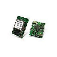
WI.232FHSS-250-R Radiotronix, WI.232FHSS-250-R Datasheet - Page 30

WI.232FHSS-250-R
Manufacturer Part Number
WI.232FHSS-250-R
Description
RF Modules & Development Tools 900MHz FHSS Low
Manufacturer
Radiotronix
Datasheet
1.WI.232FHSS-25-FCC-RA-R.pdf
(67 pages)
Specifications of WI.232FHSS-250-R
Lead Free Status / RoHS Status
Lead free / RoHS Compliant
Other names
WI232FHSS-250-R
WI.232FHSS-25-R/ WI.232FHSS-250-R DATASHEET
3.6.5. Reset (C2CK/RST)
The C2CK/RST pin is normally high. It is an open-drain input/output pin with an integrated weak pull-up.
Because it periodically operates as an output, care must be taken when interfacing to this pin. When
operating as an input, it has different functions depending on the state the module is in.
3.6.5.1. Hardware Reset (Input)
During normal operation, the pin functions as an active-low hardware reset input. When the module is
awake and running, bringing this pin low for at least 15μs forces the module’s processor into hardware
reset. While the pin is low, execution of module operations are suspended and all module I/O pins revert
to open-drain inputs with weak pull-ups. This behavior can be exploited during power-up if the V
time exceeds 1ms. By suspending execution, the dangers associated with slow V
3.6.5.2. Wake from Deep Sleep (Input)
When the module is in deep sleep, all execution is suspended in the protocol controller, and the radio is
its lowest power mode. To wake the module the module’s C2CK/RST pin must be lowered for at least
15μs. When the C2CK/RST line is raised, execution begins in the protocol controller. The module
maintains its state engine while asleep. Because of this, it can detect whether the hardware reset was
intended to cause a hard reset or wake the module. The protocol controller’s RAM is preserved during
deep sleep. The RAM is checked prior to entering deep sleep, and examined upon waking. If the RAM
contents are corrupted upon wake, the module will issue itself a software reset to reinitialize the module.
3.6.5.3. Hardware Reset Indicator (Output)
When the module starts from power-off, or is reset by the internal V
pin is driven low to indicate the reset state. During power-on reset, assuming V
C2CK/RST is driven low from the time that V
T
The other event that will drive the C2CK/RST pin low is a low-voltage or brown-out condition. In this
case, the V
until the power drops below the operating threshold for that circuit (becoming indeterminate), or until the
module power supply returns to V
output.
PORDelay
. T
DD
PORDelay
monitor will hold the device in reset, thus driving the C2CK/RST pin low. It will remain low
is the power-on reset delay imposed by the protocol controller’s hardware.
RST
. The figure below illustrates the operation of C2CK/RST as an
29
DD
reaches approximately 1V until V
DD
monitor circuitry, the C2CK/RST
DD
DD
ramp time is valid,
DD
reaches V
ramp are nullified.
Revision 1.1.0
RST
DD
+
ramp


