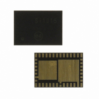
SI1015-A-GM Silicon Laboratories Inc, SI1015-A-GM Datasheet - Page 94

SI1015-A-GM
Manufacturer Part Number
SI1015-A-GM
Description
IC TXRX MCU + EZRADIOPRO
Manufacturer
Silicon Laboratories Inc
Specifications of SI1015-A-GM
Package / Case
42-QFN
Frequency
240MHz ~ 960MHz
Data Rate - Maximum
256kbps
Modulation Or Protocol
FSK, GFSK, OOK
Applications
General Purpose
Power - Output
13dBm
Sensitivity
-121dBm
Voltage - Supply
0.9 V ~ 3.6 V
Current - Receiving
18.5mA
Current - Transmitting
30mA
Data Interface
PCB, Surface Mount
Memory Size
8kB Flash, 768B RAM
Antenna Connector
PCB, Surface Mount
Number Of Receivers
1
Number Of Transmitters
1
Wireless Frequency
240 MHz to 960 MHz
Interface Type
UART, SMBus, SPI, PCA
Output Power
13 dBm
Operating Supply Voltage
0.9 V to 3.6 V
Maximum Operating Temperature
+ 85 C
Mounting Style
SMD/SMT
Maximum Supply Current
4 mA
Minimum Operating Temperature
- 40 C
Modulation
FSK, GFSK, OOK
Protocol Supported
C2, SMBus
Core
8051
Program Memory Type
Flash
Program Memory Size
8 KB
Data Ram Size
768 B
Supply Current (max)
4 mA
Lead Free Status / RoHS Status
Lead free / RoHS Compliant
Operating Temperature
-
Lead Free Status / Rohs Status
Lead free / RoHS Compliant
Other names
336-1868-5
Available stocks
Company
Part Number
Manufacturer
Quantity
Price
Company:
Part Number:
SI1015-A-GM
Manufacturer:
Silicon Labs
Quantity:
135
Part Number:
SI1015-A-GM
Manufacturer:
SILICONLA
Quantity:
20 000
- Current page: 94 of 384
- Download datasheet (3Mb)
Si1010/1/2/3/4/5
5.7. ADC0 Analog Multiplexer
ADC0 on Si1010/1/2/3/4/5 has an analog multiplexer, referred to as AMUX0.
AMUX0 selects the positive inputs to the single-ended ADC0. Any of the following may be selected as the
positive input: Port I/O pins, the on-chip temperature sensor, the VBAT Power Supply, Regulated Digital
Supply Voltage (Output of VREG0), VDD/DC+ Supply, or the positive input may be connected to GND. The
ADC0 input channels are selected in the ADC0MX register described in SFR Definition 5.12.
ADC0MX
P0.0
Programmable
Attenuator
AIN+
ADC0
AMUX
P1.6*
Temp
Sensor
Gain = 0. 5 or 1
VBAT
Digital Supply
VDD_MCU/DC+
*P1.0 – P1.3 are not
available as device pins
Figure 5.7. ADC0 Multiplexer Block Diagram
Important Note About ADC0 Input Configuration: Port pins selected as ADC0 inputs should be config-
ured as analog inputs, and should be skipped by the Digital Crossbar. To configure a Port pin for analog
input, set to 0 the corresponding bit in register PnMDIN and disable the digital driver (PnMDOUT = 0 and
Port Latch = 1). To force the Crossbar to skip a Port pin, set to 1 the corresponding bit in register PnSKIP.
See Section “21. Port Input/Output” on page 219 for more Port I/O configuration details.
94
Rev. 1.0
Related parts for SI1015-A-GM
Image
Part Number
Description
Manufacturer
Datasheet
Request
R
Part Number:
Description:
SMD/C°/SINGLE-ENDED OUTPUT SILICON OSCILLATOR
Manufacturer:
Silicon Laboratories Inc
Part Number:
Description:
Manufacturer:
Silicon Laboratories Inc
Datasheet:
Part Number:
Description:
N/A N/A/SI4010 AES KEYFOB DEMO WITH LCD RX
Manufacturer:
Silicon Laboratories Inc
Datasheet:
Part Number:
Description:
N/A N/A/SI4010 SIMPLIFIED KEY FOB DEMO WITH LED RX
Manufacturer:
Silicon Laboratories Inc
Datasheet:
Part Number:
Description:
N/A/-40 TO 85 OC/EZLINK MODULE; F930/4432 HIGH BAND (REV E/B1)
Manufacturer:
Silicon Laboratories Inc
Part Number:
Description:
EZLink Module; F930/4432 Low Band (rev e/B1)
Manufacturer:
Silicon Laboratories Inc
Part Number:
Description:
I°/4460 10 DBM RADIO TEST CARD 434 MHZ
Manufacturer:
Silicon Laboratories Inc
Part Number:
Description:
I°/4461 14 DBM RADIO TEST CARD 868 MHZ
Manufacturer:
Silicon Laboratories Inc
Part Number:
Description:
I°/4463 20 DBM RFSWITCH RADIO TEST CARD 460 MHZ
Manufacturer:
Silicon Laboratories Inc
Part Number:
Description:
I°/4463 20 DBM RADIO TEST CARD 868 MHZ
Manufacturer:
Silicon Laboratories Inc
Part Number:
Description:
I°/4463 27 DBM RADIO TEST CARD 868 MHZ
Manufacturer:
Silicon Laboratories Inc
Part Number:
Description:
I°/4463 SKYWORKS 30 DBM RADIO TEST CARD 915 MHZ
Manufacturer:
Silicon Laboratories Inc
Part Number:
Description:
N/A N/A/-40 TO 85 OC/4463 RFMD 30 DBM RADIO TEST CARD 915 MHZ
Manufacturer:
Silicon Laboratories Inc
Part Number:
Description:
I°/4463 20 DBM RADIO TEST CARD 169 MHZ
Manufacturer:
Silicon Laboratories Inc


