JN5148-001-X NXP Semiconductors, JN5148-001-X Datasheet - Page 73
JN5148-001-X
Manufacturer Part Number
JN5148-001-X
Description
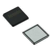
IC MCU 802.15.4 32BIT 2.4G 56QFN
Manufacturer
NXP Semiconductors
Series
JN5148r
Datasheet
1.JN5148-UG010.pdf
(99 pages)
Specifications of JN5148-001-X
Frequency
2.4GHz
Data Rate - Maximum
667kbps
Modulation Or Protocol
802.15.4
Applications
Home/Building Automation, Industrial Control
Power - Output
2.5dBm
Sensitivity
-95dBm
Voltage - Supply
2 V ~ 3.6 V
Current - Receiving
17.5mA
Current - Transmitting
15mA
Data Interface
PCB, Surface Mount
Memory Size
128kB RAM, 128kB ROM
Antenna Connector
PCB, Surface Mount
Operating Temperature
-40°C ~ 85°C
Package / Case
56-QFN
Lead Free Status / RoHS Status
Lead free / RoHS Compliant
Other names
616-1049-2
935293999531
JN5148-001-X
935293999531
JN5148-001-X


22.3.10 Comparators
VDD = 2.0 to 3.6V -40 to +85ºC
22.3.11 32kHz RC Oscillator
VDD = 2.0 to 3.6V, -40 to +85 ºC
© NXP Laboratories UK 2010
Current consumption of cell
and counter logic
32kHz clock native
accuracy
Calibrated 32kHz accuracy
Variation with temperature
Variation with VDD2
Analogue response time
(normal)
Total response time
(normal) including delay to
Interrupt controller
Analogue response time
(low power)
Hysteresis
Vref (Internal)
Common Mode input range
Current (normal mode)
Current (low power mode)
Parameter
Parameter
See Section 22.3.7 Bandgap Reference
-30%
Min
Min
12
28
54
4
0
JN-DS-JN5148-001 1v6
32kHz
-0.010
±250
1.45
1.25
1.05
Typ
-1.1
Typ
2.4
0.8
80
10
20
40
73
105 + 125
+30%
Max
Max
Vdd
125
102
16
26
50
%/°C
Unit
Unit
ppm
%/V
mV
µA
µA
µA
ns
ns
µs
V
V
+/- 250mV overdrive
10pF load
Digital delay can be
up to a max. of two
16MHz clock periods
+/- 250mV overdrive
No digital delay
Programmable in 3
steps and zero
3.6V
3.0V
2.0V
Typical is at 3.0V 25°C
For a 1 second sleep
period calibrating over
20 x 32kHz clock
periods
Notes
Notes
73
Related parts for JN5148-001-X
Image
Part Number
Description
Manufacturer
Datasheet
Request
R

Part Number:
Description:
The JN5148 is an ultra low power, high performance MCU combined with an IEEE802
Manufacturer:
NXP Semiconductors
Datasheet:

Part Number:
Description:
Microcontrollers (MCU) 32bit RISC 32MHz
Manufacturer:
NXP Semiconductors
Datasheet:
Part Number:
Description:
Microcontrollers (MCU) 32bit RISC 32MHz
Manufacturer:
NXP Semiconductors

Part Number:
Description:
Zigbee / 802.15.4 Modules & Development Tools Lo-Power RF Solution Jennic Demo Board
Manufacturer:
NXP Semiconductors
Datasheet:

Part Number:
Description:
Microcontrollers (MCU) 32bit RISC 2.4GHz
Manufacturer:
NXP Semiconductors
Datasheet:

Part Number:
Description:
MODULE ZIGBEE PRO U.FL CONN
Manufacturer:
NXP Semiconductors
Datasheet:

Part Number:
Description:
MODULE ZIGBEE PRO CERM ANTENNA
Manufacturer:
NXP Semiconductors
Datasheet:

Part Number:
Description:
MODULE ZIGBEE PRO HP U.FL CONN
Manufacturer:
NXP Semiconductors
Datasheet:

Part Number:
Description:
MCU 802.15.4 32BIT 2.4G 56-QFN
Manufacturer:
NXP Semiconductors
Datasheet:
Part Number:
Description:
MCU 802.15.4 32BIT 2.4G 56-QFN
Manufacturer:
NXP Semiconductors
Datasheet:
Part Number:
Description:
Microcontrollers (MCU) 32bit RISC 32MHz
Manufacturer:
NXP Semiconductors
Part Number:
Description:
NXP Semiconductors designed the LPC2420/2460 microcontroller around a 16-bit/32-bitARM7TDMI-S CPU core with real-time debug interfaces that include both JTAG andembedded trace
Manufacturer:
NXP Semiconductors
Datasheet:

Part Number:
Description:
NXP Semiconductors designed the LPC2458 microcontroller around a 16-bit/32-bitARM7TDMI-S CPU core with real-time debug interfaces that include both JTAG andembedded trace
Manufacturer:
NXP Semiconductors
Datasheet:
Part Number:
Description:
NXP Semiconductors designed the LPC2468 microcontroller around a 16-bit/32-bitARM7TDMI-S CPU core with real-time debug interfaces that include both JTAG andembedded trace
Manufacturer:
NXP Semiconductors
Datasheet:
Part Number:
Description:
NXP Semiconductors designed the LPC2470 microcontroller, powered by theARM7TDMI-S core, to be a highly integrated microcontroller for a wide range ofapplications that require advanced communications and high quality graphic displays
Manufacturer:
NXP Semiconductors
Datasheet: