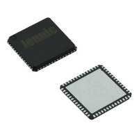
JN5148-001-X NXP Semiconductors, JN5148-001-X Datasheet - Page 46

JN5148-001-X
Manufacturer Part Number
JN5148-001-X
Description
IC MCU 802.15.4 32BIT 2.4G 56QFN
Manufacturer
NXP Semiconductors
Series
JN5148r
Datasheet
1.JN5148-UG010.pdf
(99 pages)
Specifications of JN5148-001-X
Frequency
2.4GHz
Data Rate - Maximum
667kbps
Modulation Or Protocol
802.15.4
Applications
Home/Building Automation, Industrial Control
Power - Output
2.5dBm
Sensitivity
-95dBm
Voltage - Supply
2 V ~ 3.6 V
Current - Receiving
17.5mA
Current - Transmitting
15mA
Data Interface
PCB, Surface Mount
Memory Size
128kB RAM, 128kB ROM
Antenna Connector
PCB, Surface Mount
Operating Temperature
-40°C ~ 85°C
Package / Case
56-QFN
Lead Free Status / RoHS Status
Lead free / RoHS Compliant
Other names
616-1049-2
935293999531
JN5148-001-X
935293999531
JN5148-001-X
where the hardware controls the value of the generated RTS (negated if the receive FIFO fill level is greater than a
programmable threshold of 8, 11, 13 or 15 bytes), and only transmits data when the incoming CTS is asserted.
Software can read characters, one byte at a time, from the Receive FIFO and can also write to the Transmit FIFO,
one byte at a time. The Transmit and Receive FIFOs can be cleared and reset independently of each other. The
status of the transmitter can be checked to see if it is empty, and if there is a character being transmitted. The status
of the receiver can also be checked, indicating if conditions such as parity error, framing error or break indication
have occurred. It also shows if an overrun error occurred (receive buffer full and another character arrives) and if
there is data held in the receive FIFO.
UART 0 signals CTS, RTS, TXD and RXD are alternate functions of pins DIO4, 5, 6 and 7 respectively and UART 1
signals CTS, RTS, TXD and RXD are alternate functions of pins DIO17, 18, 19 and 20 respectively. If CTS and RTS
are not required on the devices external pins, then they may be disabled, this allows the DIOx function to be used for
other purposes.
Note: With the automatic flow control threshold set to 15, the hardware flow control within the UART block negates
RTS when the receive FIFO is about to become full. In some instances it has been observed that remote devices that
are transmitting data do not respond quickly enough to the de-asserted CTS and continue to transmit data. In these
instances the data will be lost in a receive FIFO overflow.
13.1 Interrupts
Interrupt generation can be controlled for the UART block, and is divided into four categories:
•
•
•
•
13.2 UART Application
The following example shows the UART connected to a 9-pin connector compatible with a PC. As the JN5148
device pins do not provide the RS232 line voltage, a level shifter is used.
46
Received Data Available: Is set when data in the Rx FIFO queue reaches a particular level (the trigger level can
be configured as 1, 4, 8 or 14) or if no character has been received for 4 character times.
Transmit FIFO Empty: set when the last character from the Tx FIFO is read and starts to be transmitted.
Receiver Line Status: set when one of the following occur (1) Parity Error - the character at the head of the
receive FIFO has been received with a parity error, (2) Overrun Error - the Rx FIFO is full and another character
has been received at the Receiver shift register, (3) Framing Error - the character at the head of the receive
FIFO does not have a valid stop bit and (4) Break Interrupt – occurs when the RxD line has been held low for an
entire character.
Modem Status: Generated when the CTS (Clear To Send) input control line changes.
UART0
JN5148
46
44
47
45
TXD
CTS
RXD
RTS
Figure 34: JN5148 Serial Communication Link
JN-DS-JN5148-001 1v6
RS232
Shif ter
Lev el
1
6
PC COM Port
9
5
© NXP Laboratories UK 2010
Pin
1
2
3
4
5
6
7
8
9
Signal
DSR
DTR
RTS
CTS
CD
RD
TD
SG
RI


