JN5148-001-X NXP Semiconductors, JN5148-001-X Datasheet - Page 6
JN5148-001-X
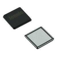
Manufacturer Part Number
JN5148-001-X
Description
IC MCU 802.15.4 32BIT 2.4G 56QFN
Manufacturer
NXP Semiconductors
Series
JN5148r
Datasheet
1.JN5148-UG010.pdf
(99 pages)
Specifications of JN5148-001-X
Frequency
2.4GHz
Data Rate - Maximum
667kbps
Modulation Or Protocol
802.15.4
Applications
Home/Building Automation, Industrial Control
Power - Output
2.5dBm
Sensitivity
-95dBm
Voltage - Supply
2 V ~ 3.6 V
Current - Receiving
17.5mA
Current - Transmitting
15mA
Data Interface
PCB, Surface Mount
Memory Size
128kB RAM, 128kB ROM
Antenna Connector
PCB, Surface Mount
Operating Temperature
-40°C ~ 85°C
Package / Case
56-QFN
Lead Free Status / RoHS Status
Lead free / RoHS Compliant
Other names
616-1049-2
935293999531
JN5148-001-X
935293999531
JN5148-001-X


1 Introduction
The JN5148-001 is an IEEE802.15.4 wireless microcontroller that provides a fully integrated solution for applications
using the IEEE802.15.4 standard in the 2.4 - 2.5GHz ISM frequency band [1], including JenNet and ZigBee PRO. It
includes all of the functionality required to meet the IEEE802.15.4, JenNet and ZigBee PRO specifications and has
additional processor capability to run a wide range of applications including, but not limited to Smart Energy,
Automatic Meter Reading, Remote Control, Home and Building Automation, Toys and Gaming.
Applications that transfer data wirelessly tend to be more complex than wired ones. Wireless protocols make
stringent demands on frequencies, data formats, timing of data transfers, security and other issues. Application
development must consider the requirements of the wireless network in addition to the product functionality and user
interfaces. To minimise this complexity, Jennic provides a series of software libraries and interfaces that control the
transceiver and peripherals of the JN5148. These libraries and interfaces remove the need for the developer to
understand wireless protocols and greatly simplifies the programming complexities of power modes, interrupts and
hardware functionality.
In view of the above, the register details of the JN5148 are not provided in the datasheet.
The device includes a Wireless Transceiver, RISC CPU, on chip memory and an extensive range of peripherals.
Hereafter, the JN5148-001 will be referred to as JN5148.
1.1 Wireless Transceiver
The Wireless Transceiver comprises a 2.45GHz radio, a modem, a baseband controller and a security coprocessor.
In addition, the radio also provides an output to control transmit-receive switching of external devices such as power
amplifiers allowing applications that require increased transmit power to be realised very easily. Appendix B.4,
describes a complete reference design including Printed Circuit Board (PCB) design and Bill Of Materials (BOM).
The security coprocessor provides hardware-based 128-bit AES-CCM* modes as specified by the IEEE802.15.4
2006 standard. Specifically this includes encryption and authentication covered by the MIC –32/ -64/ -128, ENC and
ENC-MIC –32/ -64/ -128 modes of operation.
The transceiver elements (radio, modem and baseband) work together to provide IEEE802.15.4 Medium Access
Control (MAC) under the control of a protocol stack. Applications incorporating IEEE802.15.4 functionality can be
rapidly developed by combining user-developed application software with a protocol stack library.
1.2 RISC CPU and Memory
A 32-bit RISC CPU allows software to be run on chip, its processing power being shared between the IEEE802.15.4
MAC protocol, other higher layer protocols and the user application. The JN5148 has a unified memory architecture,
code memory, data memory, peripheral devices and I/O ports are organised within the same linear address space.
The device contains 128kbytes of ROM, 128kbytes of RAM and a 32-byte One Time Programmable (OTP) eFuse
memory.
6
JN-DS-JN5148-001 1v6
© NXP Laboratories UK 2010
Related parts for JN5148-001-X
Image
Part Number
Description
Manufacturer
Datasheet
Request
R

Part Number:
Description:
The JN5148 is an ultra low power, high performance MCU combined with an IEEE802
Manufacturer:
NXP Semiconductors
Datasheet:

Part Number:
Description:
Microcontrollers (MCU) 32bit RISC 32MHz
Manufacturer:
NXP Semiconductors
Datasheet:
Part Number:
Description:
Microcontrollers (MCU) 32bit RISC 32MHz
Manufacturer:
NXP Semiconductors

Part Number:
Description:
Zigbee / 802.15.4 Modules & Development Tools Lo-Power RF Solution Jennic Demo Board
Manufacturer:
NXP Semiconductors
Datasheet:

Part Number:
Description:
Microcontrollers (MCU) 32bit RISC 2.4GHz
Manufacturer:
NXP Semiconductors
Datasheet:

Part Number:
Description:
MODULE ZIGBEE PRO U.FL CONN
Manufacturer:
NXP Semiconductors
Datasheet:

Part Number:
Description:
MODULE ZIGBEE PRO CERM ANTENNA
Manufacturer:
NXP Semiconductors
Datasheet:

Part Number:
Description:
MODULE ZIGBEE PRO HP U.FL CONN
Manufacturer:
NXP Semiconductors
Datasheet:

Part Number:
Description:
MCU 802.15.4 32BIT 2.4G 56-QFN
Manufacturer:
NXP Semiconductors
Datasheet:
Part Number:
Description:
MCU 802.15.4 32BIT 2.4G 56-QFN
Manufacturer:
NXP Semiconductors
Datasheet:
Part Number:
Description:
Microcontrollers (MCU) 32bit RISC 32MHz
Manufacturer:
NXP Semiconductors
Part Number:
Description:
NXP Semiconductors designed the LPC2420/2460 microcontroller around a 16-bit/32-bitARM7TDMI-S CPU core with real-time debug interfaces that include both JTAG andembedded trace
Manufacturer:
NXP Semiconductors
Datasheet:

Part Number:
Description:
NXP Semiconductors designed the LPC2458 microcontroller around a 16-bit/32-bitARM7TDMI-S CPU core with real-time debug interfaces that include both JTAG andembedded trace
Manufacturer:
NXP Semiconductors
Datasheet:
Part Number:
Description:
NXP Semiconductors designed the LPC2468 microcontroller around a 16-bit/32-bitARM7TDMI-S CPU core with real-time debug interfaces that include both JTAG andembedded trace
Manufacturer:
NXP Semiconductors
Datasheet:
Part Number:
Description:
NXP Semiconductors designed the LPC2470 microcontroller, powered by theARM7TDMI-S core, to be a highly integrated microcontroller for a wide range ofapplications that require advanced communications and high quality graphic displays
Manufacturer:
NXP Semiconductors
Datasheet: