JN5148-001-X NXP Semiconductors, JN5148-001-X Datasheet - Page 47
JN5148-001-X
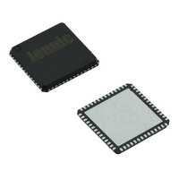
Manufacturer Part Number
JN5148-001-X
Description
IC MCU 802.15.4 32BIT 2.4G 56QFN
Manufacturer
NXP Semiconductors
Series
JN5148r
Datasheet
1.JN5148-UG010.pdf
(99 pages)
Specifications of JN5148-001-X
Frequency
2.4GHz
Data Rate - Maximum
667kbps
Modulation Or Protocol
802.15.4
Applications
Home/Building Automation, Industrial Control
Power - Output
2.5dBm
Sensitivity
-95dBm
Voltage - Supply
2 V ~ 3.6 V
Current - Receiving
17.5mA
Current - Transmitting
15mA
Data Interface
PCB, Surface Mount
Memory Size
128kB RAM, 128kB ROM
Antenna Connector
PCB, Surface Mount
Operating Temperature
-40°C ~ 85°C
Package / Case
56-QFN
Lead Free Status / RoHS Status
Lead free / RoHS Compliant
Other names
616-1049-2
935293999531
JN5148-001-X
935293999531
JN5148-001-X


14 JTAG Debug Interface
The JN5148 includes an IEEE1149.1 compliant JTAG port for the sole purpose of software code debug with Jennic's
Software Development Kit. The JTAG interface is disabled by default and is enabled under software control.
Therefore, debugging is only possible if enabled by the application. Once enabled, the application executes as
normal until the external debugger controller initiates debug activity.
The Debugger supports breakpoints and watchpoints based on four comparisons between any of program counter,
load/store effective address and load/store data. There is the ability to chain the comparisons together. There is also
the ability, under debugger control to perform the following commands: go, stop, reset, step over/into/out/next, run to
cursor and breakpoints. In addition, under control of the debugger, it is possible to:
•
•
•
The Debugger interface is accessed, depending upon the configuration, through the pins used for UART0 or UART1.
This is enabled under software control and is dealt with in JN-AN-1118 JN5148 Application Debugging [4]. The
following table details which DIO are used for the JTAG interface depending upon the configuration.
If doze mode is active when debugging is started, the processor will be woken and then respond to debugger
commands. It is not possible to wake the device from sleep using the debug interface and debugging is not available
while the device is sleeping.
When using the debug interface, program execution is halted, and control of the CPU is handed to the debugger. The
watchdog, tick timer and the three timers described in section 11 are stalled while the debugger is in control of the
CPU.
When control is handed from the CPU to the debugger or back a small number of CPU clock cycles are taken
flushing or reloading the CPU pipeline. Because of this, when a program is halted by the debugger and then restarted
again, a small number of tick timer cycles will elapse.
It is possible to prevent all hardware debugging by blowing the relevant Efuse bit.
The JTAG interface does not support boundary scan testing. It is recommended that the JN5148 is not connected as
part of the board scan chain.
© NXP Laboratories UK 2010
Read and write registers on the wishbone bus
Read ROM and RAM, and write to RAM
Read and write CPU internal registers
Signal
data out (TDO)
control (TMS)
data in (TDI)
clock (TCK)
Table 4 Hardware Debugger IO
JN-DS-JN5148-001 1v6
UART0 pins
4
5
6
7
DIO Assignment
UART1 pins
17
18
19
20
47
Related parts for JN5148-001-X
Image
Part Number
Description
Manufacturer
Datasheet
Request
R

Part Number:
Description:
The JN5148 is an ultra low power, high performance MCU combined with an IEEE802
Manufacturer:
NXP Semiconductors
Datasheet:

Part Number:
Description:
Microcontrollers (MCU) 32bit RISC 32MHz
Manufacturer:
NXP Semiconductors
Datasheet:
Part Number:
Description:
Microcontrollers (MCU) 32bit RISC 32MHz
Manufacturer:
NXP Semiconductors

Part Number:
Description:
Zigbee / 802.15.4 Modules & Development Tools Lo-Power RF Solution Jennic Demo Board
Manufacturer:
NXP Semiconductors
Datasheet:

Part Number:
Description:
Microcontrollers (MCU) 32bit RISC 2.4GHz
Manufacturer:
NXP Semiconductors
Datasheet:

Part Number:
Description:
MODULE ZIGBEE PRO U.FL CONN
Manufacturer:
NXP Semiconductors
Datasheet:

Part Number:
Description:
MODULE ZIGBEE PRO CERM ANTENNA
Manufacturer:
NXP Semiconductors
Datasheet:

Part Number:
Description:
MODULE ZIGBEE PRO HP U.FL CONN
Manufacturer:
NXP Semiconductors
Datasheet:

Part Number:
Description:
MCU 802.15.4 32BIT 2.4G 56-QFN
Manufacturer:
NXP Semiconductors
Datasheet:
Part Number:
Description:
MCU 802.15.4 32BIT 2.4G 56-QFN
Manufacturer:
NXP Semiconductors
Datasheet:
Part Number:
Description:
Microcontrollers (MCU) 32bit RISC 32MHz
Manufacturer:
NXP Semiconductors
Part Number:
Description:
NXP Semiconductors designed the LPC2420/2460 microcontroller around a 16-bit/32-bitARM7TDMI-S CPU core with real-time debug interfaces that include both JTAG andembedded trace
Manufacturer:
NXP Semiconductors
Datasheet:

Part Number:
Description:
NXP Semiconductors designed the LPC2458 microcontroller around a 16-bit/32-bitARM7TDMI-S CPU core with real-time debug interfaces that include both JTAG andembedded trace
Manufacturer:
NXP Semiconductors
Datasheet:
Part Number:
Description:
NXP Semiconductors designed the LPC2468 microcontroller around a 16-bit/32-bitARM7TDMI-S CPU core with real-time debug interfaces that include both JTAG andembedded trace
Manufacturer:
NXP Semiconductors
Datasheet:
Part Number:
Description:
NXP Semiconductors designed the LPC2470 microcontroller, powered by theARM7TDMI-S core, to be a highly integrated microcontroller for a wide range ofapplications that require advanced communications and high quality graphic displays
Manufacturer:
NXP Semiconductors
Datasheet: