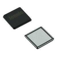
JN5148-001-X NXP Semiconductors, JN5148-001-X Datasheet - Page 40

JN5148-001-X
Manufacturer Part Number
JN5148-001-X
Description
IC MCU 802.15.4 32BIT 2.4G 56QFN
Manufacturer
NXP Semiconductors
Series
JN5148r
Datasheet
1.JN5148-UG010.pdf
(99 pages)
Specifications of JN5148-001-X
Frequency
2.4GHz
Data Rate - Maximum
667kbps
Modulation Or Protocol
802.15.4
Applications
Home/Building Automation, Industrial Control
Power - Output
2.5dBm
Sensitivity
-95dBm
Voltage - Supply
2 V ~ 3.6 V
Current - Receiving
17.5mA
Current - Transmitting
15mA
Data Interface
PCB, Surface Mount
Memory Size
128kB RAM, 128kB ROM
Antenna Connector
PCB, Surface Mount
Operating Temperature
-40°C ~ 85°C
Package / Case
56-QFN
Lead Free Status / RoHS Status
Lead free / RoHS Compliant
Other names
616-1049-2
935293999531
JN5148-001-X
935293999531
JN5148-001-X
9
5
3
4
CLK
CAPT
t
t
RISE
RISE
t
FALL
Capture Mode Enabled
Rise
x
9
3
Fall
x
14
7
Figure 28: Capture Mode
11.1.3 Counter/Timer Mode
The counter/timer can be used to generate interrupts, based on the timers or event counting, for software to use. As
a timer the clock source is from the system clock, prescaled if required. The timer period is programmed into the Fall
register and the Fall register match interrupt enabled. The timer is started as either a single-shot or a repeating timer,
and generates an interrupt when the counter reaches the Fall register value.
When used to count external events on TIMxCK_GT the clock source is selected from the input pin and the number
of events programmed into the Fall register. The Fall register match interrupt is enabled and the counter started,
usually in single shot mode. An interrupt is generated when the programmed number of transitions is seen on the
input pin. The transitions counted can configured to be rising, falling or both rising and falling edges.
Edges on the event signal must be at least 100nsec apart, i.e. pulses must be wider than 100nsec.
11.1.4 Delta-Sigma Mode
A separate delta-sigma mode is available, allowing a low speed delta-sigma DAC to be implemented with up to 16-bit
resolution. This requires that a resistor-capacitor network is placed between the output DIO pin and digital ground. A
stream of pulses with digital voltage levels is generated which is integrated by the RC network to give an analogue
voltage. A conversion time is defined in terms of a number of clock cycles. The width of the pulses generated is the
period of a clock cycle. The number of pulses output in the cycle, together with the integrator RC values, will
determine the resulting analogue voltage. For example, generating approximately half the number of pulses that
make up a complete conversion period will produce a voltage on the RC output of VDD1/2, provided the RC time
constant is chosen correctly. During a conversion, the pulses will be pseudo-randomly dispersed throughout the
cycle in order to produce a steady voltage on the output of the RC network.
The output signal is asserted for the number of clock periods defined in the High register, with the total period being
16
2
cycles. For the same value in the High register, the pattern of pulses on subsequent cycles is different, due to the
pseudo-random distribution.
The delta-sigma convertor output can operate in a Return-To-Zero (RTZ) or a Non-Return-to-Zero (NRZ) mode. The
NRZ mode will allow several pulses to be output next to each other. The RTZ mode ensures that each pulse is
separated from the next by at least one period. This improves linearity if the rise and fall times of the output are
different to one another. Essentially, the output signal is low on every other output clock period, and the conversion
17
cycle time is twice the NRZ cycle time ie 2
clocks. The integrated output will only reach half VDD2 in RTZ mode,
since even at full scale only half the cycle contains pulses. Figure 29 and Figure 30 illustrate the difference between
RTZ and NRZ for the same programmed number of pulses.
40
JN-DS-JN5148-001 1v6
© NXP Laboratories UK 2010


