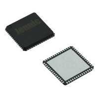
JN5148-001-X NXP Semiconductors, JN5148-001-X Datasheet - Page 49

JN5148-001-X
Manufacturer Part Number
JN5148-001-X
Description
IC MCU 802.15.4 32BIT 2.4G 56QFN
Manufacturer
NXP Semiconductors
Series
JN5148r
Datasheet
1.JN5148-UG010.pdf
(99 pages)
Specifications of JN5148-001-X
Frequency
2.4GHz
Data Rate - Maximum
667kbps
Modulation Or Protocol
802.15.4
Applications
Home/Building Automation, Industrial Control
Power - Output
2.5dBm
Sensitivity
-95dBm
Voltage - Supply
2 V ~ 3.6 V
Current - Receiving
17.5mA
Current - Transmitting
15mA
Data Interface
PCB, Surface Mount
Memory Size
128kB RAM, 128kB ROM
Antenna Connector
PCB, Surface Mount
Operating Temperature
-40°C ~ 85°C
Package / Case
56-QFN
Lead Free Status / RoHS Status
Lead free / RoHS Compliant
Other names
616-1049-2
935293999531
JN5148-001-X
935293999531
JN5148-001-X
15.2 Clock Stretching
Slave devices can use clock stretching to slow down the transfer bit rate. After the master has driven SIF_CLK low,
the slave can drive SIF_CLK low for the required period and then release it. If the slave’s SIF_CLK low period is
greater than the master’s low period the resulting SIF_CLK bus signal low period is stretched thus inserting wait
states.
15.3 Master Two-wire Serial Interface
When operating as a master device, it provides the clock signal and a prescale register determines the clock rate,
allowing operation up to 400kbit/s.
Data transfer is controlled from the processor bus interface at a byte level, with the processor responsible for
indicating when start, stop, read, write and acknowledge control should be generated. Write data written into a
transmit buffer will be written out across the two-wire interface when indicated, and read data received on the
interface is made available in a receive buffer. Indication of when a particular transfer has completed may be
indicated by means of an interrupt or by polling a status bit.
The first byte of data transferred by the device after a start bit is the slave address. The JN5148 supports both 7-bit
and 10-bit slave addresses by generating either one or two address transfers. Only the slave with a matching address
will respond by returning an acknowledge bit.
The master interface provides a true multi-master bus including collision detection and arbitration that prevents data
corruption. If two or more masters simultaneously try to control the bus, a clock synchronization procedure
determines the bus clock. Because of the wired-AND connection of the interface, a high-to-low transition on the bus
affects all connected devices. This means a high-to-low transition on the SIF_CLK line causes all concerned devices
to count off their low period. Once the clock input of a device has gone low, it will hold the SIF_CLK line in that state
until the clock high state is reached when it releases the SIF_CLK line. Due to the wired-AND connection, the
SIF_CLK line will therefore be held low by the device with the longest low period, and held high by the device with the
shortest high period.
After each transfer has completed, the status of the device must be checked to ensure that the data has been
acknowledged correctly, and that there has been no loss of arbitration. (N.B. Loss of arbitration may occur at any
point during the transfer, including data cycles). An interrupt will be generated when arbitration has been lost.
© NXP Laboratories UK 2010
SIF_CLK1
SIF_CLK2
SIF_CLK
SIF_CLK
SIF_CLK
SIF_CLK
Figure 37: Multi-Master Clock Synchronisation
Start counting
low period
Figure 36: Clock Stretching
JN-DS-JN5148-001 1v6
Clock held low
by Slave
State
Wait
Start counting
high period
Master SIF_CLK
Slave SIF_CLK
Wired-AND SIF_CLK
Master1 SIF_CLK
Master2 SIF_CLK
Wired-AND SIF_CLK
49


