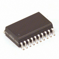
MC68HC908JB8JDW Freescale Semiconductor, MC68HC908JB8JDW Datasheet - Page 61

MC68HC908JB8JDW
Manufacturer Part Number
MC68HC908JB8JDW
Description
IC MCU 8K FLASH 3MHZ 20-SOIC
Manufacturer
Freescale Semiconductor
Series
HC08r
Datasheet
1.MC908JB8JDWE.pdf
(286 pages)
Specifications of MC68HC908JB8JDW
Core Processor
HC08
Core Size
8-Bit
Speed
3MHz
Connectivity
USB
Peripherals
LVD, POR, PWM
Number Of I /o
13
Program Memory Size
8KB (8K x 8)
Program Memory Type
FLASH
Ram Size
256 x 8
Voltage - Supply (vcc/vdd)
4 V ~ 5.5 V
Oscillator Type
Internal
Operating Temperature
0°C ~ 70°C
Package / Case
20-SOIC (7.5mm Width)
Lead Free Status / RoHS Status
Contains lead / RoHS non-compliant
Eeprom Size
-
Data Converters
-
Available stocks
Company
Part Number
Manufacturer
Quantity
Price
Part Number:
MC68HC908JB8JDW
Manufacturer:
MOTOROLA/摩托罗拉
Quantity:
20 000
Company:
Part Number:
MC68HC908JB8JDWE
Manufacturer:
VISHAY
Quantity:
6 700
Part Number:
MC68HC908JB8JDWE
Manufacturer:
FREESCALE
Quantity:
20 000
- Current page: 61 of 286
- Download datasheet (2Mb)
4.9 ROM-Resident Routines
MC68HC908JB8•MC68HC08JB8•MC68HC08JT8 — Rev. 2.3
Freescale Semiconductor
ROM-resident routines can be called by a program running in user mode
or in monitor mode (see
programming, erasing, and verifying. The range of the FLASH memory
must be unprotected (see
erase or programming routine.
BPR0 is used only for BPR[7:0] = $FF, for no block protection.
The resultant 16-bit address is used for specifying the start address
of the FLASH memory for block protection. The FLASH is protected
from this start address to the end of FLASH memory, at $FFFF. With
this mechanism, the protect start address can be X000, X200, X400,
X600, X800, XA00, XC00, or XE00 within the FLASH memory.
Examples of protect start address:
PROGRAM
Routine
VERIFY
ERASE
Name
and so on...
Note:
The end address of the protected range is always $FFFF.
$DE (1101 1110)
$E0 (1110 0000)
$E2 (1110 0010)
$E4 (1110 0100)
$00 to $DC
BPR[7:0]
$FE
$FF
FLASH Memory
Table 4-1. ROM-Resident Routines
Call Address
$FC03
$FC06
$FC09
Section 10. Monitor ROM
4.8 FLASH
The entire FLASH memory is not protected.
FLASH verify routine
FLASH mass erase routine
FLASH program routine
The entire FLASH memory is protected.
Start of Address of Protect Range
$DE00 (1101 1110 0000 0000)
$E000 (1110 0000 0000 0000)
$E200 (1110 0010 0000 0000)
$E400 (1110 0100 0000 0000)
$FFE0–$FFFF (User vectors)
Protection) before calling the
Routine Function
ROM-Resident Routines
(MON)) for FLASH
FLASH Memory
Technical Data
61
Related parts for MC68HC908JB8JDW
Image
Part Number
Description
Manufacturer
Datasheet
Request
R
Part Number:
Description:
Manufacturer:
Freescale Semiconductor, Inc
Datasheet:
Part Number:
Description:
Manufacturer:
Freescale Semiconductor, Inc
Datasheet:
Part Number:
Description:
Manufacturer:
Freescale Semiconductor, Inc
Datasheet:
Part Number:
Description:
Manufacturer:
Freescale Semiconductor, Inc
Datasheet:
Part Number:
Description:
Manufacturer:
Freescale Semiconductor, Inc
Datasheet:
Part Number:
Description:
Manufacturer:
Freescale Semiconductor, Inc
Datasheet:
Part Number:
Description:
Manufacturer:
Freescale Semiconductor, Inc
Datasheet:
Part Number:
Description:
Manufacturer:
Freescale Semiconductor, Inc
Datasheet:
Part Number:
Description:
Manufacturer:
Freescale Semiconductor, Inc
Datasheet:
Part Number:
Description:
Manufacturer:
Freescale Semiconductor, Inc
Datasheet:
Part Number:
Description:
Manufacturer:
Freescale Semiconductor, Inc
Datasheet:
Part Number:
Description:
Manufacturer:
Freescale Semiconductor, Inc
Datasheet:
Part Number:
Description:
Manufacturer:
Freescale Semiconductor, Inc
Datasheet:
Part Number:
Description:
Manufacturer:
Freescale Semiconductor, Inc
Datasheet:
Part Number:
Description:
Manufacturer:
Freescale Semiconductor, Inc
Datasheet:


