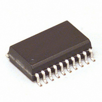
MC68HC908JB8JDW Freescale Semiconductor, MC68HC908JB8JDW Datasheet - Page 206

MC68HC908JB8JDW
Manufacturer Part Number
MC68HC908JB8JDW
Description
IC MCU 8K FLASH 3MHZ 20-SOIC
Manufacturer
Freescale Semiconductor
Series
HC08r
Datasheet
1.MC908JB8JDWE.pdf
(286 pages)
Specifications of MC68HC908JB8JDW
Core Processor
HC08
Core Size
8-Bit
Speed
3MHz
Connectivity
USB
Peripherals
LVD, POR, PWM
Number Of I /o
13
Program Memory Size
8KB (8K x 8)
Program Memory Type
FLASH
Ram Size
256 x 8
Voltage - Supply (vcc/vdd)
4 V ~ 5.5 V
Oscillator Type
Internal
Operating Temperature
0°C ~ 70°C
Package / Case
20-SOIC (7.5mm Width)
Lead Free Status / RoHS Status
Contains lead / RoHS non-compliant
Eeprom Size
-
Data Converters
-
Available stocks
Company
Part Number
Manufacturer
Quantity
Price
Part Number:
MC68HC908JB8JDW
Manufacturer:
MOTOROLA/摩托罗拉
Quantity:
20 000
Company:
Part Number:
MC68HC908JB8JDWE
Manufacturer:
VISHAY
Quantity:
6 700
Part Number:
MC68HC908JB8JDWE
Manufacturer:
FREESCALE
Quantity:
20 000
- Current page: 206 of 286
- Download datasheet (2Mb)
Input/Output Ports (I/O)
Technical Data
206
When bit DDRBx is a logic 1, reading address $0001 reads the PTBx
data latch. When bit DDRBx is a logic 0, reading address $0001 reads
the voltage level on the pin. The data latch can always be written,
regardless of the state of its data direction bit.
the operation of the port B pins.
NOTES:
1. X = don’t care.
2. Hi-Z = high impedance.
3. Writing affects data register, but does not affect input.
DDRB
Bit
0
1
READ DDRB ($0005)
WRITE DDRB ($0005)
WRITE PTB ($0001)
READ PTB ($0001)
PTB Bit
Input/Output Ports (I/O)
X
X
(1)
Table 12-3. Port B Pin Functions
Figure 12-7. Port B I/O Circuit
MC68HC908JB8•MC68HC08JB8•MC68HC08JT8 — Rev. 2.3
RESET
I/O Pin Mode
Input, Hi-Z
Output
(2)
DDRBx
PTBx
Read/Write
DDRB[7:0]
DDRB[7:0]
Accesses
to DDRB
Table 12-3
PTB[7:0]
Freescale Semiconductor
Read
Accesses to PTB
Pin
summarizes
PTB[7:0]
PTB[7:0]
Write
PTBx
(3)
Related parts for MC68HC908JB8JDW
Image
Part Number
Description
Manufacturer
Datasheet
Request
R
Part Number:
Description:
Manufacturer:
Freescale Semiconductor, Inc
Datasheet:
Part Number:
Description:
Manufacturer:
Freescale Semiconductor, Inc
Datasheet:
Part Number:
Description:
Manufacturer:
Freescale Semiconductor, Inc
Datasheet:
Part Number:
Description:
Manufacturer:
Freescale Semiconductor, Inc
Datasheet:
Part Number:
Description:
Manufacturer:
Freescale Semiconductor, Inc
Datasheet:
Part Number:
Description:
Manufacturer:
Freescale Semiconductor, Inc
Datasheet:
Part Number:
Description:
Manufacturer:
Freescale Semiconductor, Inc
Datasheet:
Part Number:
Description:
Manufacturer:
Freescale Semiconductor, Inc
Datasheet:
Part Number:
Description:
Manufacturer:
Freescale Semiconductor, Inc
Datasheet:
Part Number:
Description:
Manufacturer:
Freescale Semiconductor, Inc
Datasheet:
Part Number:
Description:
Manufacturer:
Freescale Semiconductor, Inc
Datasheet:
Part Number:
Description:
Manufacturer:
Freescale Semiconductor, Inc
Datasheet:
Part Number:
Description:
Manufacturer:
Freescale Semiconductor, Inc
Datasheet:
Part Number:
Description:
Manufacturer:
Freescale Semiconductor, Inc
Datasheet:
Part Number:
Description:
Manufacturer:
Freescale Semiconductor, Inc
Datasheet:


