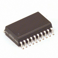
MC68HC908JB8JDW Freescale Semiconductor, MC68HC908JB8JDW Datasheet - Page 37

MC68HC908JB8JDW
Manufacturer Part Number
MC68HC908JB8JDW
Description
IC MCU 8K FLASH 3MHZ 20-SOIC
Manufacturer
Freescale Semiconductor
Series
HC08r
Datasheet
1.MC908JB8JDWE.pdf
(286 pages)
Specifications of MC68HC908JB8JDW
Core Processor
HC08
Core Size
8-Bit
Speed
3MHz
Connectivity
USB
Peripherals
LVD, POR, PWM
Number Of I /o
13
Program Memory Size
8KB (8K x 8)
Program Memory Type
FLASH
Ram Size
256 x 8
Voltage - Supply (vcc/vdd)
4 V ~ 5.5 V
Oscillator Type
Internal
Operating Temperature
0°C ~ 70°C
Package / Case
20-SOIC (7.5mm Width)
Lead Free Status / RoHS Status
Contains lead / RoHS non-compliant
Eeprom Size
-
Data Converters
-
Available stocks
Company
Part Number
Manufacturer
Quantity
Price
Part Number:
MC68HC908JB8JDW
Manufacturer:
MOTOROLA/摩托罗拉
Quantity:
20 000
Company:
Part Number:
MC68HC908JB8JDWE
Manufacturer:
VISHAY
Quantity:
6 700
Part Number:
MC68HC908JB8JDWE
Manufacturer:
FREESCALE
Quantity:
20 000
- Current page: 37 of 286
- Download datasheet (2Mb)
MC68HC908JB8•MC68HC08JB8•MC68HC08JT8 — Rev. 2.3
Freescale Semiconductor
PTB0–PTB7
PTA0/KBA0
PTA7/KBA7
PIN NAME
OSC1
OSC2
V
RST
V
IRQ
V
REG
DD
SS
:
Power supply.
Power supply ground.
Regulated 3.3V output from MCU.
Reset input; active low.
With internal pullup to V
External IRQ pin; with programmable internal pullup to V
and schmitt trigger input.
Used for mode entry selection.
Crystal oscillator input.
Crystal oscillator output; inverting of OSC1 signal.
8-bit general-purpose I/O port.
Pins as keyboard interrupts, KBA0–KBA7.
Each pin has programmable internal pullup to V
configured as input.
8-bit general-purpose I/O port.
Each pin has programmable internal pullup to V
configured as input.
When the USB module is disabled, the PTE4 and PTE3 pins are
general-purpose bidirectional I/O port pins with 10mA sink capability.
Each pin is open-drain when configured as an output; and each pin
contains a software configurable 5kΩ pullup to V
an input. The PTE4 pin can also be enabled to trigger the IRQ interrupt.
When the USB module is enabled, the PTE4/D– and PTE3/D+ pins
become the USB module D– and D+ pins. The D– pin contains a
software configurable 1.5kΩ pullup to V
Interface Module
(USB)
Summary of the pin functions are provided in
Table 1-1. Summary of Pin Functions
and
PIN DESCRIPTION
DD
Section 12. Input/Output Ports
and schmitt trigger input.
General Description
(TIM),
Section 9. Universal Serial Bus Module
REG
REG
when
when
DD
REG
. (See
(I/O).)
IN/OUT
IN/OUT
IN/OUT
IN/OUT
Table
OUT
OUT
OUT
IN
IN
IN
IN
IN
IN
IN
DD
Section 11. Timer
when configured as
1-1.
VOLTAGE LEVEL
General Description
V
REG
V
Pin Assignments
4.0 to 5.5V
REG
Technical Data
to V
V
V
V
V
V
V
V
V
V
0V
REG
REG
REG
REG
REG
REG
REG
DD
DD
(3.3V)
DD
+V
HI
37
Related parts for MC68HC908JB8JDW
Image
Part Number
Description
Manufacturer
Datasheet
Request
R
Part Number:
Description:
Manufacturer:
Freescale Semiconductor, Inc
Datasheet:
Part Number:
Description:
Manufacturer:
Freescale Semiconductor, Inc
Datasheet:
Part Number:
Description:
Manufacturer:
Freescale Semiconductor, Inc
Datasheet:
Part Number:
Description:
Manufacturer:
Freescale Semiconductor, Inc
Datasheet:
Part Number:
Description:
Manufacturer:
Freescale Semiconductor, Inc
Datasheet:
Part Number:
Description:
Manufacturer:
Freescale Semiconductor, Inc
Datasheet:
Part Number:
Description:
Manufacturer:
Freescale Semiconductor, Inc
Datasheet:
Part Number:
Description:
Manufacturer:
Freescale Semiconductor, Inc
Datasheet:
Part Number:
Description:
Manufacturer:
Freescale Semiconductor, Inc
Datasheet:
Part Number:
Description:
Manufacturer:
Freescale Semiconductor, Inc
Datasheet:
Part Number:
Description:
Manufacturer:
Freescale Semiconductor, Inc
Datasheet:
Part Number:
Description:
Manufacturer:
Freescale Semiconductor, Inc
Datasheet:
Part Number:
Description:
Manufacturer:
Freescale Semiconductor, Inc
Datasheet:
Part Number:
Description:
Manufacturer:
Freescale Semiconductor, Inc
Datasheet:
Part Number:
Description:
Manufacturer:
Freescale Semiconductor, Inc
Datasheet:


