CY7C60223-PXC Cypress Semiconductor Corp, CY7C60223-PXC Datasheet - Page 45
CY7C60223-PXC
Manufacturer Part Number
CY7C60223-PXC
Description
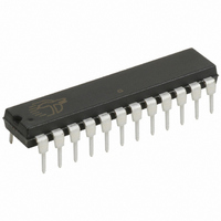
IC MCU 8K WIRELESS 24-DIP
Manufacturer
Cypress Semiconductor Corp
Series
enCoRe™ II CY7C602xxr
Datasheet
1.CY7C60123-PVXC.pdf
(68 pages)
Specifications of CY7C60223-PXC
Core Processor
M8C
Core Size
8-Bit
Speed
12MHz
Connectivity
SPI
Peripherals
LVD, POR, WDT
Number Of I /o
20
Program Memory Size
8KB (8K x 8)
Program Memory Type
FLASH
Ram Size
256 x 8
Voltage - Supply (vcc/vdd)
2.7 V ~ 3.6 V
Oscillator Type
Internal
Operating Temperature
0°C ~ 70°C
Package / Case
24-DIP (0.300", 7.62mm)
For Use With
770-1001 - ISP 4PORT CYPRESS ENCORE II MCUCY3216 - KIT PROGRAMMER MODULAR428-1774 - EXTENSION KIT FOR ENCORE II428-1773 - KIT DEVELOPMENT ENCORE II
Lead Free Status / RoHS Status
Lead free / RoHS Compliant
Eeprom Size
-
Data Converters
-
Other names
428-1797
Available stocks
Company
Part Number
Manufacturer
Quantity
Price
Company:

Part Number:
CY7C60223-PXC
Manufacturer:
TEXAS
Quantity:
93


17.1 SPI Data Register
Table 17-1. SPI Data Register (SPIDATA) [0x3C] [R/W]
When an interrupt occurs to indicate to firmware that a byte of receive data is available or the transmitter holding register is empty,
firmware has seven SPI clocks to manage the buffers—to empty the receiver buffer or to refill the transmit holding register. Failure to
meet this timing requirement results in incorrect data transfer.
17.2 SPI Configure Register
Table 17-2. SPI Configure Register (SPICR) [0x3D] [R/W]
Document 38-16016 Rev. *F
When read, this register returns the contents of the receive buffer. When written, it loads the transmit holding register.
Bit [7:0]: SPI Data [7:0]
Bit 7: Swap
0 = Swap function disabled
1 = The SPI block swaps its use of SMOSI and SMISO. Among other things, this is useful to implement single wire communi-
cations similar to SPI.
Bit 6: LSB First
0 = The SPI transmits and receives the MSB (Most Significant Bit) first.
1 = The SPI transmits and receives the LSB (Least Significant Bit) first.
Bit [5:4]: Comm Mode [1:0]
0 0: All SPI communication disabled
0 1: SPI master mode
1 0: SPI slave mode
1 1: Reserved
Bit 3: CPOL
This bit controls the SPI clock (SCLK) idle polarity.
0 = SCLK idles low
1 = SCLK idles high
Bit 2: CPHA
The Clock Phase bit controls the phase of the clock on which data is sampled.
combinations of LSB First, CPOL, and CPHA.
Bit [1:0]: SCLK Select
This field selects the speed of the master SCLK. When in master mode, SCLK is generated by dividing the base CPUCLK
Important Note for Comm Modes 01b or 10b (SPI Master or SPI Slave)
When configured for SPI, (SPI Use = 1 –
is set automatically by the SPI logic. However, pin P1.4's input and output direction is NOT automatically set; it must be explic-
itly set by firmware. For SPI Master mode, pin P1.4 is configured as an output; for SPI Slave mode, pin P1.4 is configured as
an input.
Read/Write
Read/Write
Default
Default
Field
Field
Bit #
Bit #
Swap
R/W
R/W
7
0
7
0
LSB First
R/W
R/W
6
0
6
0
Table 16-10
R/W
R/W
5
0
5
0
Comm Mode
on page 42), the input and output direction of pins P1.3, P1.5, and P1.6
R/W
R/W
4
0
4
0
SPIData[7:0]
CPOL
R/W
R/W
Table 17-3
3
0
3
0
on page 46 shows the timing for various
CPHA
R/W
R/W
CY7C601xx, CY7C602xx
2
0
2
0
R/W
R/W
1
0
1
0
SCLK Select
Page 45 of 68
R/W
R/W
0
0
0
0
[+] Feedback
Related parts for CY7C60223-PXC
Image
Part Number
Description
Manufacturer
Datasheet
Request
R

Part Number:
Description:
Manufacturer:
Cypress Semiconductor Corp
Datasheet:
Part Number:
Description:
Manufacturer:
Cypress Semiconductor Corp
Datasheet:
Part Number:
Description:
Manufacturer:
Cypress Semiconductor Corp
Datasheet:
Part Number:
Description:
Manufacturer:
Cypress Semiconductor Corp
Datasheet:
Part Number:
Description:
Manufacturer:
Cypress Semiconductor Corp
Datasheet: