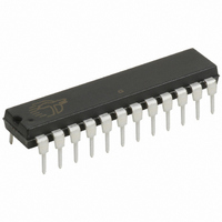
CY7C60223-PXC Cypress Semiconductor Corp, CY7C60223-PXC Datasheet - Page 37

CY7C60223-PXC
Manufacturer Part Number
CY7C60223-PXC
Description
IC MCU 8K WIRELESS 24-DIP
Manufacturer
Cypress Semiconductor Corp
Series
enCoRe™ II CY7C602xxr
Datasheet
1.CY7C60123-PVXC.pdf
(68 pages)
Specifications of CY7C60223-PXC
Core Processor
M8C
Core Size
8-Bit
Speed
12MHz
Connectivity
SPI
Peripherals
LVD, POR, WDT
Number Of I /o
20
Program Memory Size
8KB (8K x 8)
Program Memory Type
FLASH
Ram Size
256 x 8
Voltage - Supply (vcc/vdd)
2.7 V ~ 3.6 V
Oscillator Type
Internal
Operating Temperature
0°C ~ 70°C
Package / Case
24-DIP (0.300", 7.62mm)
For Use With
770-1001 - ISP 4PORT CYPRESS ENCORE II MCUCY3216 - KIT PROGRAMMER MODULAR428-1774 - EXTENSION KIT FOR ENCORE II428-1773 - KIT DEVELOPMENT ENCORE II
Lead Free Status / RoHS Status
Lead free / RoHS Compliant
Eeprom Size
-
Data Converters
-
Other names
428-1797
Available stocks
Company
Part Number
Manufacturer
Quantity
Price
Company:
Part Number:
CY7C60223-PXC
Manufacturer:
TEXAS
Quantity:
93
16.1.3 P2 Data
Table 16-3. P2 Data Register (P2DATA) [0x02] [R/W]
16.1.4 P3 Data
Table 16-4. P3 Data Register (P3DATA) [0x03] [R/W]
16.1.5 P4 Data
Table 16-5. P4 Data Register (P4DATA) [0x04] [R/W]
16.2 GPIO Port Configuration
All GPIO configuration registers have common configuration
controls. By default all GPIOs are configured as inputs. To
prevent the inputs from floating, pull up resistors are enabled.
Firmware configures each of the GPIOs before use. The
following are bit definitions of the GPIO configuration registers.
16.2.1 Int Enable
When set, the Int Enable bit allows the GPIO to generate inter-
rupts. Interrupt generate occurs regardless of whether the pin is
configured for input or output. All interrupts are edge sensitive.
However, for interrupts that are shared by multiple sources
(Ports 2, 3, and 4), all inputs are deasserted before a new
interrupt occurs.
When clear, the corresponding interrupt is disabled on the pin.
Document 38-16016 Rev. *F
This register contains the data for Port 2. Writing to this register sets the bit values to be output on output enabled pins. Reading
from this register returns the current state of the Port 2 pins.
Bit [7:2]: P2 Data [7:2]
Bit [1:0]: P2 Data [1:0]
This register contains the data for Port 3. Writing to this register sets the bit values to be output on output enabled pins. Reading
from this register returns the current state of the Port 3 pins.
Bit [7:2]: P3 Data [7:2]
Bit [1:0]: P3 Data [1:0]
This register contains the data for Port 4. Writing to this register sets the bit values to be output on output enabled pins. Reading
from this register returns the current state of the Port 2 pins.
Bit [7:4]: Reserved
Bit [3:0]: P4 Data [3:0]
P4.3–P4.0 only exist in the CY7C601xx.
Read/Write
Read/Write
Read/Write
Default
Default
Default
Field
Field
Field
Bit #
Bit #
Bit #
R/W
R/W
7
0
7
0
7
–
0
R/W
R/W
6
0
6
0
6
–
0
Reserved
R/W
R/W
5
0
5
0
5
–
0
P2.7–P2.2
P3.7–P3.2
R/W
R/W
4
0
4
0
4
–
0
It is possible to configure GPIOs as outputs, enable the interrupt
on the pin, and then generate the interrupt by driving the appro-
priate pin state. This is useful in test and may find value in appli-
cations as well.
16.2.2 Int Act Low
When clear, the corresponding interrupt is active HIGH. When
set, the interrupt is active LOW. For P0.2–P0.4 Int Act Low
makes interrupts active on the rising edge. Int Act Low set makes
interrupts active on the falling edge.
16.2.3 TTL Thresh
When set, the input has TTL threshold. When clear, the input has
standard CMOS threshold.
Note The GPIOs default to CMOS threshold. User’s firmware
needs to configure the threshold to TTL mode if necessary.
R/W
R/W
R/W
3
0
3
0
3
0
R/W
R/W
R/W
CY7C601xx, CY7C602xx
2
0
2
0
2
0
P4.3–P4.0
R/W
R/W
R/W
1
0
1
0
1
0
P2.1–P2.0
P3.1–P3.0
Page 37 of 68
R/W
R/W
R/W
0
0
0
0
0
0
[+] Feedback


